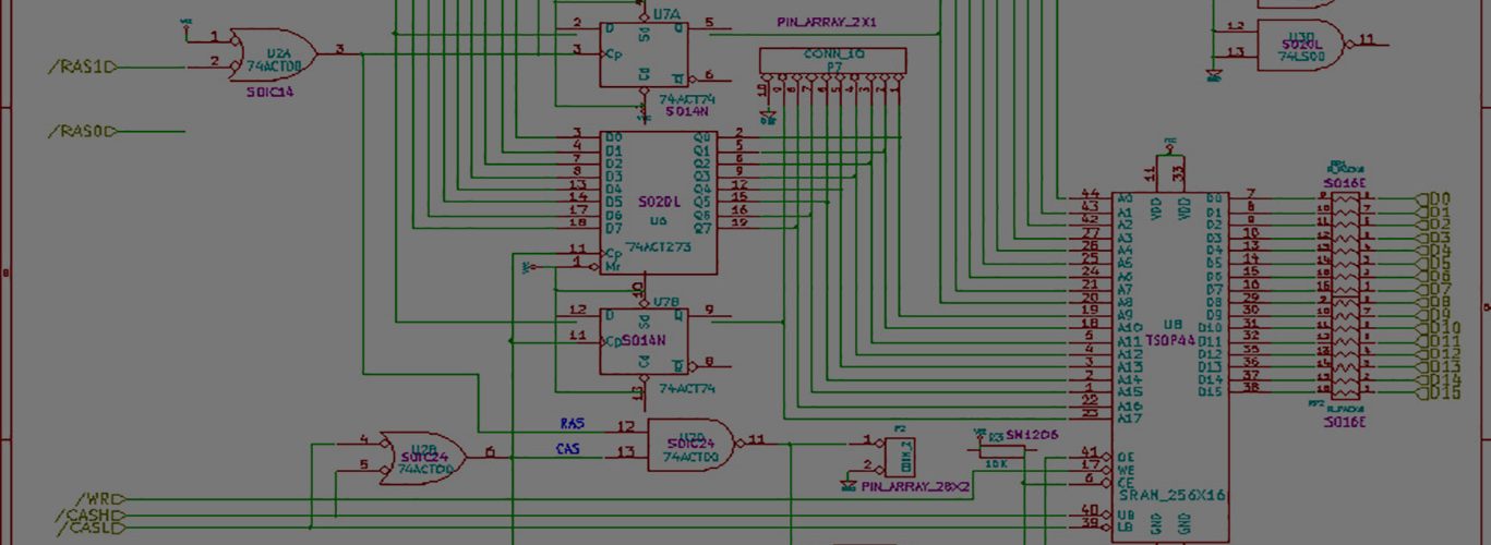
I want to put together a softcore 68K computer system, just something simple.
I’ve purchased, but not yet received, the Terasic Cyclone V GX Starter Kit, an Altera FPGA eval board.
It looks pretty sweet and includes some fun stuff I’ve never done like HDMI connectors, has some easy to access onboard SRAM, has built in FTDI USB support, built in programmer, built-in flash for non-volatile storage, 77K logic elements, and the list goes on. Looks like a really sweet board EXCEPT for one line on the datasheet:
4Gb LPDDR2 x32 bits data bus
“Oh no! Not yet a different memory chip or interface”
What’s nice is that there are (2) HARD memory controllers built-in to the FPGA, and so you don’t have to waste logic elements for defining your own. While I’m not sure what I was thinking, I really expected the interface to the memory to be very simple…. You know something like a FIFO-front end where you’d specific address, read/write, data, and then throw some read_data_valid switch and voila. Well, of course, I’m wrong.
Again, I’m in the middle of a memory controller nightmare.
For my Altera DE0, I modified the memory controller found here. It works like a champ, and the interface is pretty darn simple.
I could really use some help putting together a simple to use DDR2 controller to access this chip:
MT42L128M32D1LF-25 WT
It’s configured like this: 16 Meg x 32 x 8 banks x 1 die. Rows are addressed like this “16K (A[13:0])” and columns “1K (A[9:0])” using Single Channel Addressing. Cycle Time is “-25 = 2.5ns, tCK RL = 6”
What I don’t know is whether I can even start with a SDRAM controller and then expand on that, or if a completely different approach is warranted. I know that DDR2 is still SDRAM, and the interface to the new memory chip is very similar. I don’t really need the double-pumping or the increased data rate — I’d take anything to get off the ground.
Ideally, I’d find a verilog module for a controller with an example module that instantiates it, writes to some addresses, and then reads them back and verifies them.
A google search, as well as investigation on OpenCores hasn’t yielded much. This Altera youtube video is promising, but it stopped short on showing the HDL-specific details on how to instantiate it, and how to actually USE the module that gets created. This is assuming that everything goes swimmingly during the fairly complicated MegaWizard process.
If you’ve got any experience or helpful tips, I’d appreciate it.


Hello Keith,
I should work on an LPDDR2 controller in the near future. I will keep you posted on this.
Micron has a verilog model with a working testbench (I ran it under Active-HDL without any trouble), this will give you some idea about the initialization sequence.
Also, keep in mind that the LPDDR2 can run at very low speed (down to 10 MHz), this can be useful for retro gaming project and you do not have to worry too much about leveling, termination, etc… at that speed.
Regards,
Frederic
Frederic,
Thanks for the post.
I might be outsourcing (see elance.com) a memory controller produced exactly to my specifications….. I’d release it as open source. I want something dead simple to operate with a very easy interface.
I’m more interested in the projects I can build with an easy to use memory controller versus worrying about the minute details of getting a memory controller right.
The Altera UniPHY IP hard memory controller uses something like 7000 slices (3000 ALMs) and seems overkill to me in many ways. I thought the idea of using a hard controller was to save logic space?
What do you think are the key requirements for a memory controller? Run at full speed? (in this case, 400mhz clock) Support burst mode? Support multiple ports? What should I be sure to include?
Thanks
You just got caught in the modern FPGA & boards. (neither Altera or Xilinx care how many LUTs or whatever you have to use this days). DDRx works really very different to the SDRAM you know, so get a fresh start. If you like somebody else to write it (elance.com, etc…) specify simply, that you like to have a SRAM like interface, which should be capable of 8/16/32 bit accesses.
So he will write some DDRx interface with a cache in between, to translate all the weird bursts of DDRx, into the cache, take care of filling/emptying the caches, and you get some SRAM like interface with Data_Vaild signals, and wait, or …
But on the other side, Altera should provide some application notes, or building block for access of DDRx RAM, right? What’s wrong with them?
Cheers
Here’s a link to the job description I posted on elance.com. I’d link to the job directly, but it has been awarded, so the accessibility might change.
https://techtravels.org/wp-content/uploads/2015/07/Terms.txt
I did exactly what you suggested — specified a sram-like interface. But I’d appreciate a review of my specifications/requirements. If only for the next time I do this type of thing. I think I covered most bases.
My main issues with Altera’s controller are:
1. The controller is a big fat pig. It’s about 3000 ALMs, which is about 10% of my device. Yes, it’s not that much, but heck it’s 50% of my previous eval board. It sounds like way too much.
2. The megafunction wizard is a pig too. It takes a loong time to even generate the core and example code.
3. Compiling the core automatically adds almost (15) minutes to every design that includes it. This doesn’t even include my “regular” main application logic. Given that I’m somewhat of a trial-and-error guy, I often do tiny tweaks here and there to see, “Did I fix it? No? How about now? No? How about this? ok got it.” Having long compiling times TAXES each change individually. That sucks.
4. Did I mention it was a pig? Hundreds of files and something like 30,000-40,000 lines of HDL. The process isn’t THAT complicated, is it?
5. This point has more to do with my lack of knowledge/skills than anything, but the avalon-mm as a front-end isn’t exactly straight-forward to me. Now I’ve never used it before, so this might just be ignorance. I’ve used SRAMs and blockrams/m9k’s, distributed ram, and those are pieces of cake to setup and use.
I’ve done perhaps a 1/2 dozen different FPGA designs, that have all eventually worked, but this is a common problem for me. The interfaces are almost always overkill for what I need, and I never know what part is the “minimum-required” to make it work. I need a dummies guide to hardware front-ends. Those wizards aren’t all horrible, and I often find myself disabling any unnecessary inputs/outputs (like when creating a FIFO) and that simplifies things enough to get the core idea working.
I’m going to build a new 4-ghz (Quad core, or maybe 8-core) PC with a buttload of RAM installed, and potentially a raided SSD. I need to throw more hardware at this FPGA compiling business.
Thanks for the post.
Hello Keith,
good that you found somebody who will do the job, hopefully he is knowledgeable enough to do it right ; -) You specification is good enough to have a start, if you work with him during the development, you should be able to get a satisfying result …
I know it complicates things, but I probably would have thrown in a open source 32bit CPU to see, how the core behaves …
to the points you made, please bear with me, I’m a Xilinx user myself, but it is interesting, that they are pretty similar in the direction they are going 😉
1.) completely agree. I used DDR3 before, it was a walk in the park and performance was nice. The memory controller & the multiport was well hidden, and didn’t use that much resources. Now on the 7 series, it uses quite a lot of the resources, so the smaller chips are not really usable anymore for serious work with DDR3.
2.) but it produces working results, doesn’t it? 😉
3.) Hopefully, you are doing something wrong there. It should offer some “incremental” synthesis/etc. so it doesn’t get touched on every compile …
4.) actually, it is pretty complicated to do it right. But it could have been done in Hardware, but they didn’t 🙁
5.) I thought altera went to AXI (instead of avalon, which was easier) too?
Prepare yourself to spend a lot of time in the simulator in the future 😉
Cheers & good luck!