 --
--
A501 512K DRAM Card Redesign Project
So in my overall quest to understand more about the Commodore Amiga 500, I decided just recently to take on a new project. I want to build a replacement A501 512K memory expansion trapdoor card. Not a sidecar memory expansion. Not even a 1MB version or larger version(yet). Just a straight-up simple A501 replacement.
Now, I know this has been done before, but I'd like to make my own. It doesn't seem like there is very much documentation on the A500 DRAM memory controller located in Agnus as far as things like Data Setup and Hold, the type of refreshes, and all the necessary details.
I've attached my HP Logic Analyzer to an A500, and sniffing the connection that goes to a Rev 5 A501. I've figured out what is happening, and I'll tell the story and give logic analyzer traces to show exactly how this external card functions.
As with many of my projects, I've solicited help from online in terms of requesting documentation, advice from people much more knowledgeable than I, and just overall guidance. No one has helped more than Mingy! This guy is a genius, and I'm happy to have someone who really knows his stuff help me out. Thanks Mingy!!
I'll provide an updated summary here, along with the traces I've captured here. I'll be using blog posts to detail the day by day efforts which have already begun.....
Project Goals
- Learn how the Amiga trapdoor 512K expansion memory system works. What makes it tick? How often does it tick?

- Create glue logic that connects a DRAM controller(Agnus) to a SRAM memory chip
- Create a prototype solderless breadboard version that works.
- Use cheap, modern components that are available off-the-shelf from Digi-Key or similar.
- Create a PCB that matches the form factor (probably much smaller) than the original.
- Provide all the necessary technical details online, for free -- hopefully doing a better job than I've done before on previous projects.

- Speed up overall development, because I think my projects take too long.
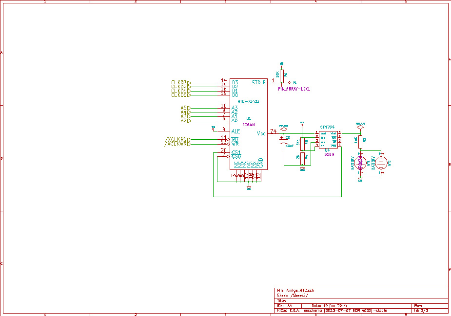
- Incorporate the real-time clock to the design.
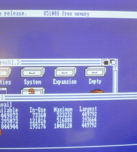
Project Summary: As of 1/11/14, the PCB is working exactly as designed! Active timeframe on the project was approximately October 2013-January 2014!
Next Steps: Continued testing of the prototype. Get more information online.
Observations
- The Amiga looks like it sends RAS-only refreshes. I don't see CAS-Before-RAS, Hidden refreshes, Pin-1 Refreshes (no such thing on the LH21256 chips anyways) and so on.
- PIns 37 and 38 on the 56-pin male dual-row header are switched in the A500 Plus Service manual. This means that /XRAS0 (the Row Address Strobe for the internal 512K RAM) is actually on pin 37. So /XRAS1 (the Row Address Strobe for the trapdoor 512K RAM) is actually on pin 38. There is a jumper(actually just pads) on the motherboard that control which one is which.....which probably explains the differences. This pad is called JP3 and located directly to the right of the top most soldered-in DRAM chip on the motherboard.
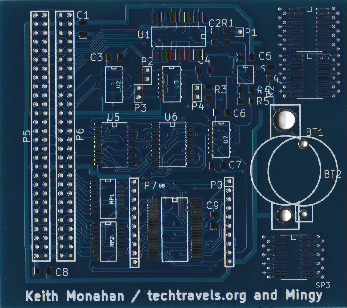
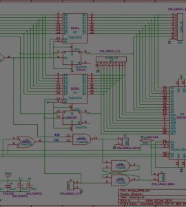
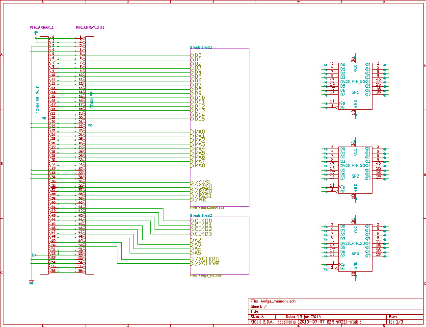
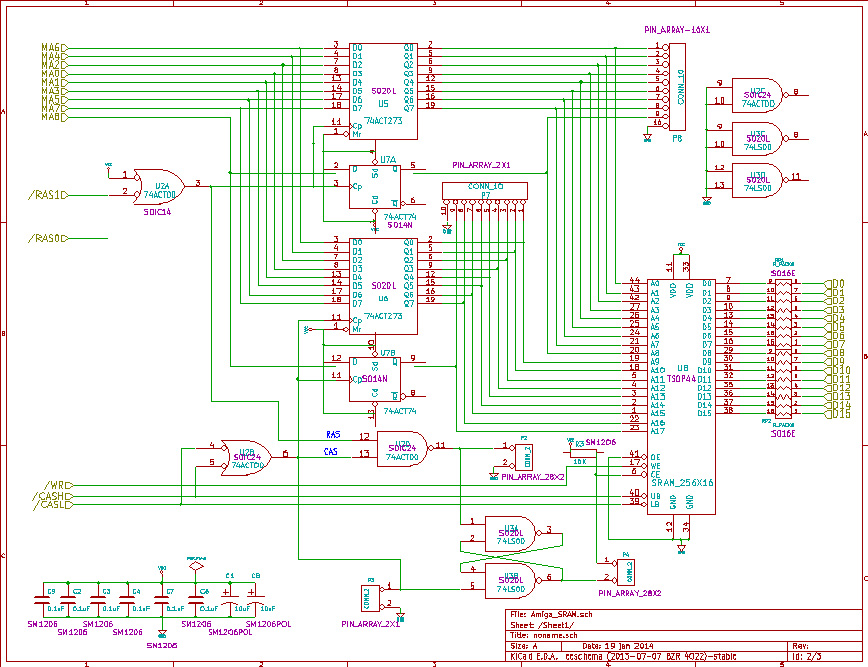
Schematic
This is a multiple page schematic. The first page is an overall schematic. The second page contains the main design, including the so-called glue logic for converting RAS/CAS's into Chip Enable's for the SRAM. The last page contains the RTC design.
Full Hi-Res Schematics in a PDF. Download here.

What will you make available? See my answer on this comment.
Why did you use SRAM instead of DRAM?
Good question. The main issue was finding low-cost 5v-compatible 256k 16-bit width(wider chips have many more pins and more complicated to solder packages) DRAM available in single-unit quantities available from a normal supplier. The real time clock I use is a $6+ chip, which is the most expensive component of the whole project. At the time, no DRAM chips at Digikey, Mouser, or Newark fit the bill. I searched a few weeks ago, and found exactly (1) chip marked as Legacy, having no current datasheet available, that cost around $13.00 each. One of the stated project goals is using off-the-shelf modern components, and the less than $4.50 ISSI SRAM fit nicely. Besides, the additional complexity required for the glue logic, in terms of the added logic design components (and cost), and PCB size was pretty minor --- and a lot of fun figuring out the best approach. 'Nuff said on this.
Logic Analyzer Traces
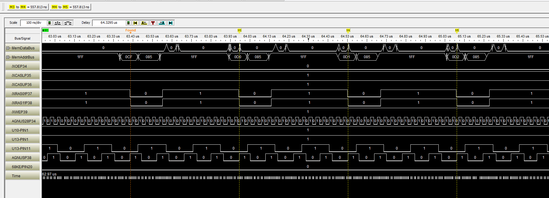
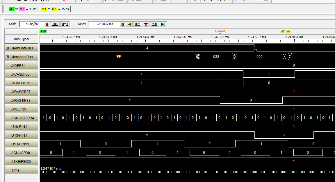
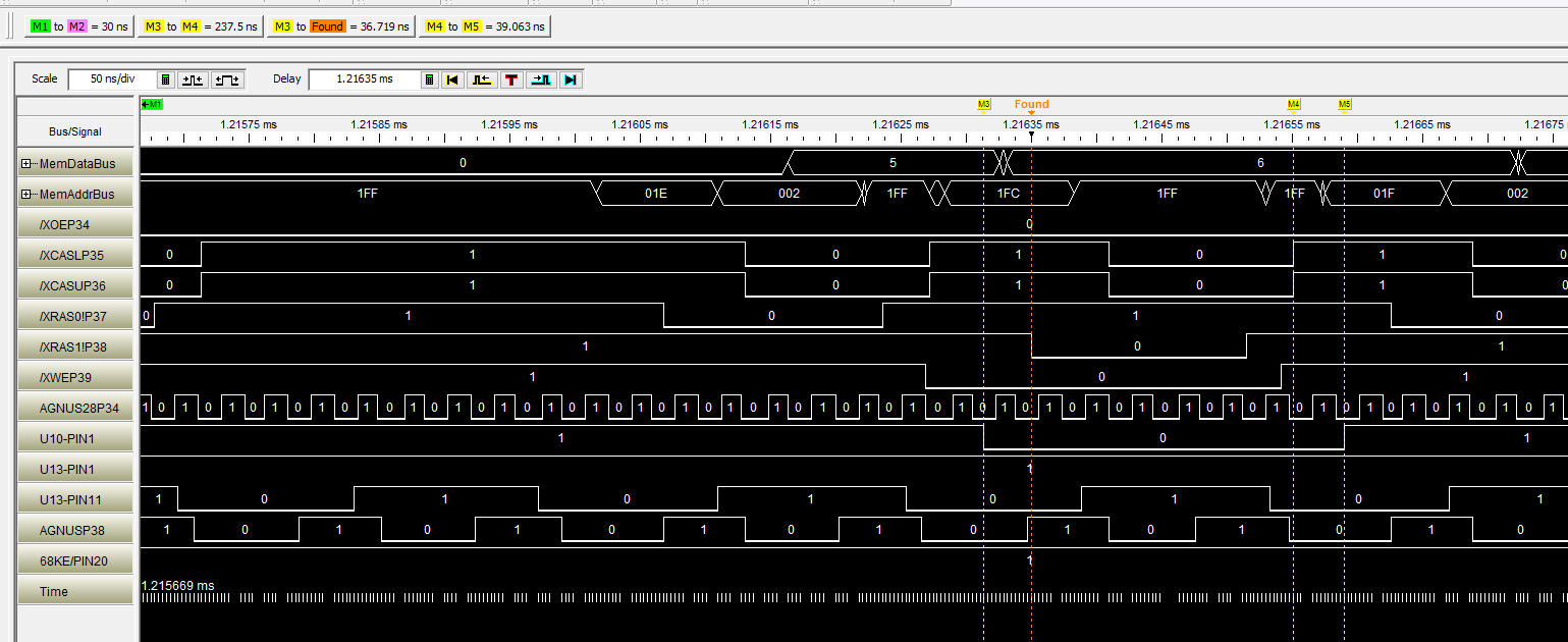
This one below shows RAS-only refreshes happening. Notice how the ROW address(0CF, 0D0, 0D1) keeps incrementing. Also notice that both the internal RAS0, and external RAS1 refreshes happen at the same time.
RAS's are negative going pulses, usually about 168ns wide, and the memory uses it to latch the incoming ROW Address. Each row needs accessed (either by a refresh, or by a normal access) within some fixed period of time. These refreshes are separated by 557.813ns. The CAS address shows 0x085 but is really irrelevant because it is simply not used. The RAS and CAS addresses are 9 bits wide.
The falling edge is nicely centered on the row address. And also notice that the rising edge of the clock on Agnus Pin 38, the ~7mhz clock. -- The falling edge of RAS is synchronous with it.
This next one below shows the read timing. I'll add some more description when I find the time.
This shows some writes happening.
The image below shows the internal operation of a write cycle on the new PCB. The write cycle is critical because we need to ensure that the incoming latched column address is stable prior to dropping /CE, respecting the Address Setup Time requirements of the SRAM.
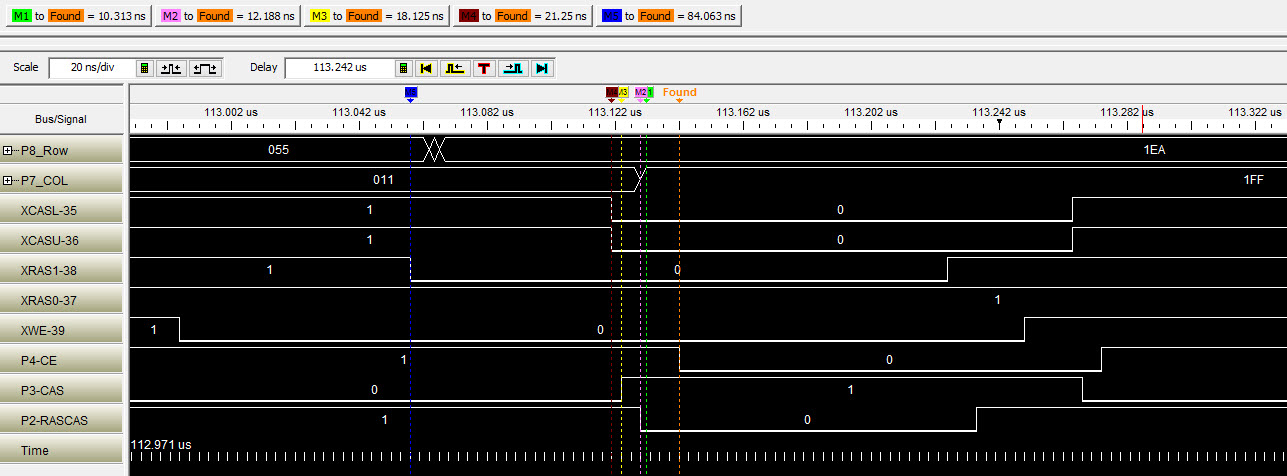
M5 Blue Line: /RAS falls. Notice that /XWE is already setup, so we know this is a write cycle. This causes the row address to latch, in P8 above.
M4 Red Line: Both CASs fall which indicate a full 16-bit WORD write instead of a BYTE write.
M3 Yellow Line: Glue logic reacts to the /CAS edge and causes the column address to be latched.
M2 Purple Line: Both our R and S inputs to our LS00 SR NAND latch have been satisfied to cause /CE to drop. In order to slow this latch down to give additional time for our address bus to settle, I moved this from 74ACT logic to 74LS logic to INCREASE the propagation time.
M1 Green Line: The bus is settled. This happens around 10ns before /CE falls.
Found Brown Line: /CE is forced low, bringing the SRAM active.
More information like parts list, and theory of operation will be coming. (wrote this 2/22/14)
RTC Traces
The trace below shows a write occurring during the AmigaDos command "setclock save." The address bus(XA) shows that a "1-minute register" write is occurring, because register "2" is associated with that position. The value being written was an "8", so the time was 21:58, or 21:48, or 21:38...you get the picture.
What confuses me is why we see a double-write? The register is first zero'd out, but then another write-cycle occurs and writes the correct "8" into it. This seems odd, please get in touch with me if you know the answer! I'd love to look at the source of setclock or commented (dis)assembly.
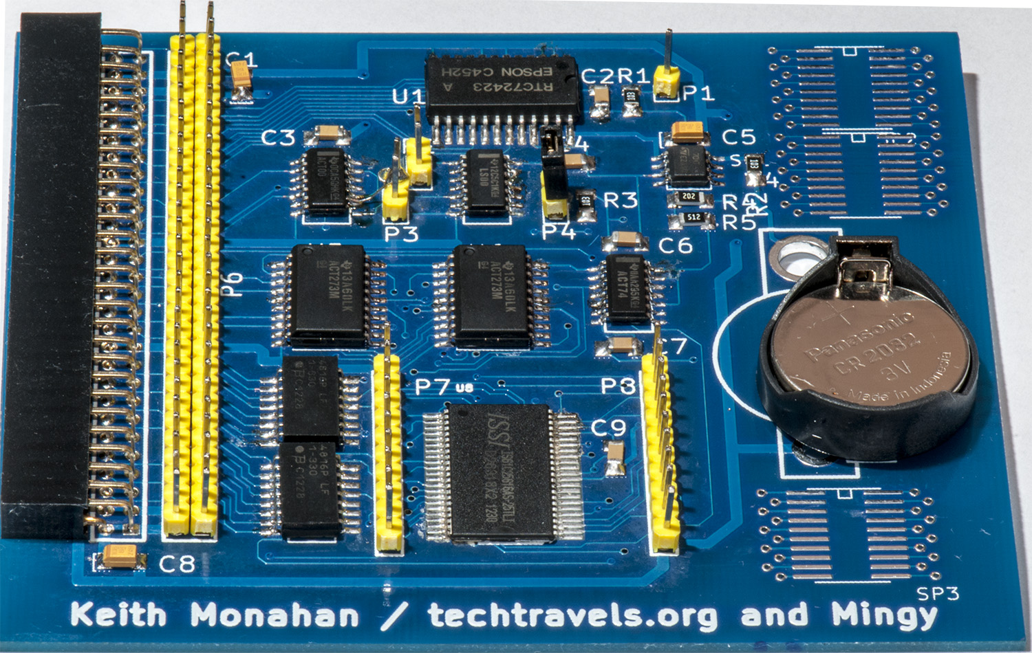
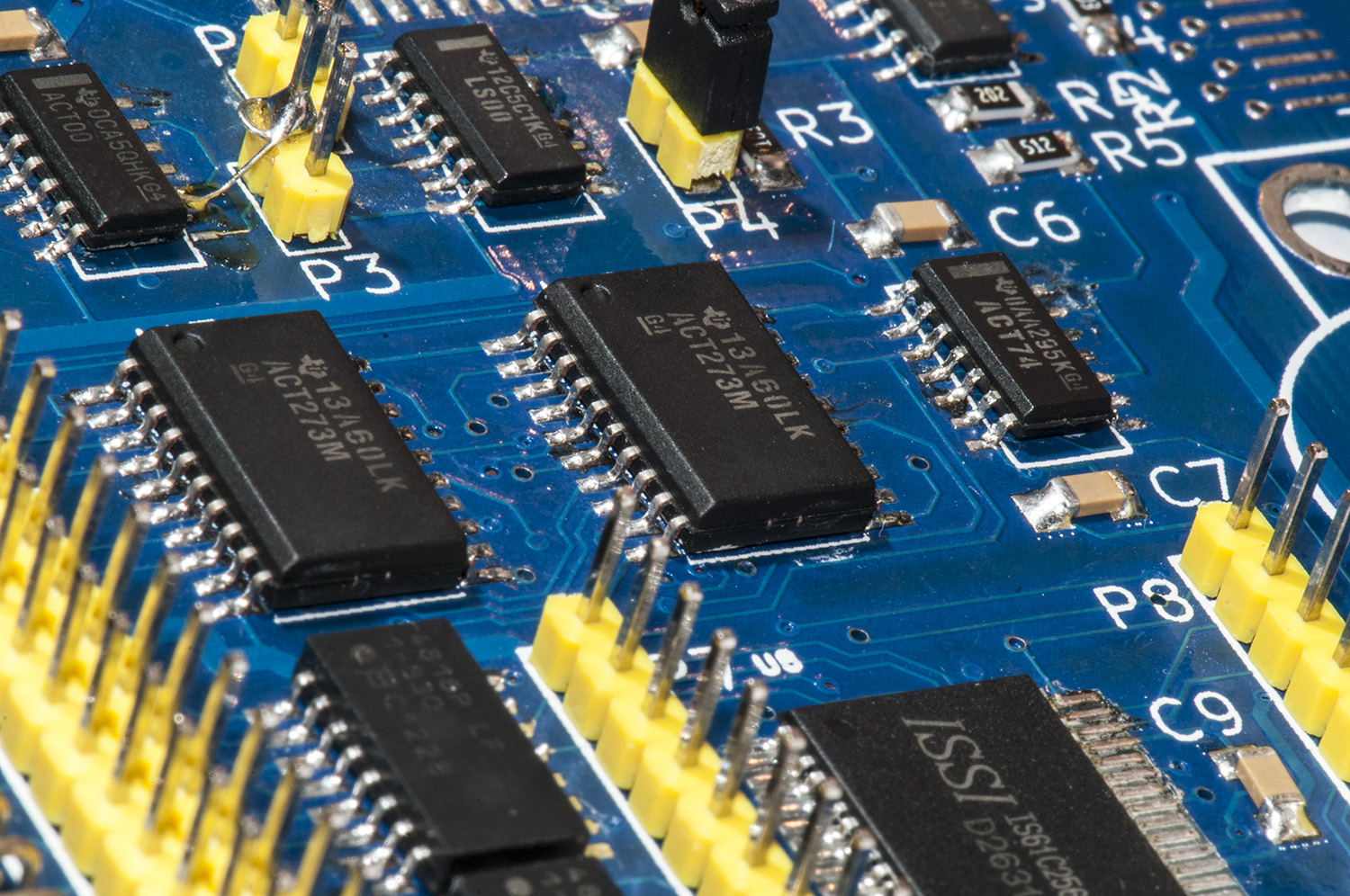
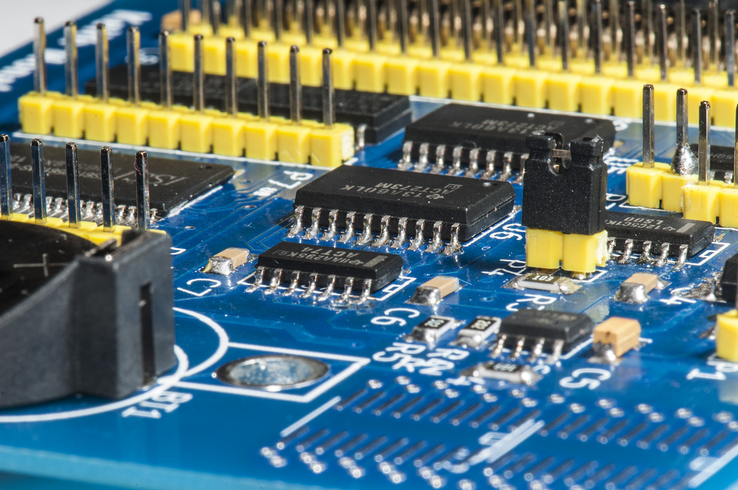
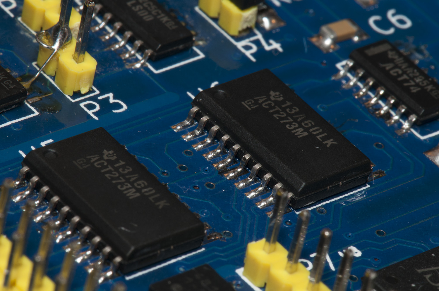
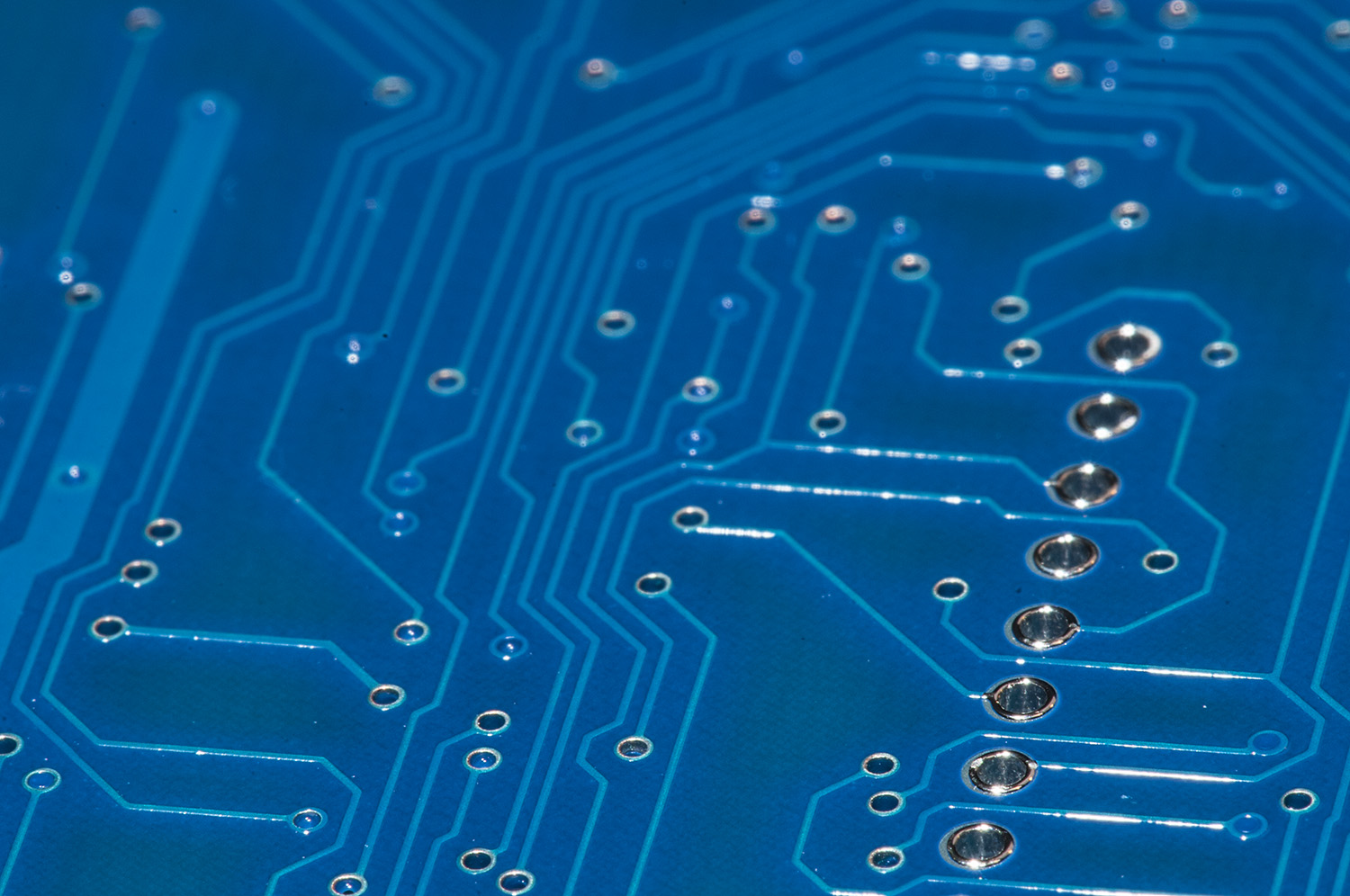
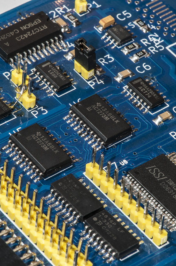
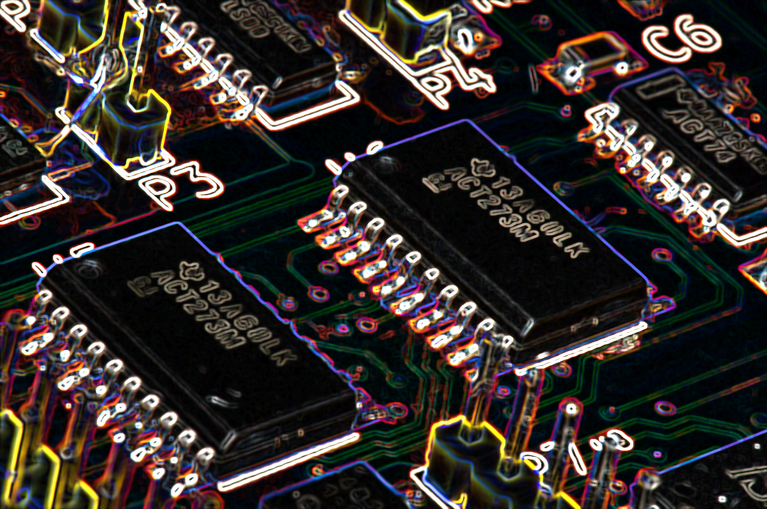
Photos
These were shot with a Nikon D300 with the AF-S VR Micro-Nikkor 105mm f/2.8G IF-ED lens with off-camera lighting, including an SB700 mounted on a tripod. They were mostly shot handheld! Most were done at ISO200, f/32, 1/60s. This lens is pretty sharp, and allowed me to get in really close, within 5 or 6 inches of the PCB from the front of lens. I'm not thrilled with my overall composition skills, but they work for me.