About
Hi, I’m Keith Monahan — a lifelong electronics tinkerer, retro-computing enthusiast, and relentless debugger of both code and hardware. I grew up on the Commodore Amiga 500, and while many of the projects on this site still revolve around that legendary machine, techtravels has grown into something broader: a modern hub for reverse engineering, hardware hacking, and deep dives into vintage and contemporary tech.
My curiosity started young — often at the expense of my toys. I’d take them apart to understand how they worked, much to my dad’s dismay. My first real exposure to electronics came through the iconic Radio Shack books by Forrest M. Mims III. I experimented with 555 timers and simple circuits, but in the ’80s, the complexity of discrete electronics kept me at bay. For a while, I stuck to software — proudly anti-hardware.
That changed in 2005 when I resurrected my Amiga and thousands of old floppy disks. Frustrated by modern PC limitations with the Amiga format, I dove headfirst into building a custom hardware and software solution to read and preserve my old data. That project — involving Parallax microcontrollers, Xilinx FPGAs, and custom Java code — became the Amiga Floppy Project Blog, my first real foray into combining retro tech with modern tools.
Today, I work professionally in software quality assurance, putting my obsessive attention to detail to good use by catching bugs before users ever see them (and occasionally annoying a developer or two in the process). I also explore logic analyzers, signal tracing, GAL/PAL reverse engineering, and building hardware tools that support vintage computing — often with a focus on learning, experimentation, and documenting the journey.
Outside of tech, I’m a proud husband and dad. My kids’ endless curiosity reminds me of my own — back when I was popping open toys just to see what was inside.
And yeah — I’m a hacker. In almost every sense of the word.
Contact
I’m always excited to hear from people and can be reached by simply emailing the same domain you’re on now and putting my first name before AT symbol.
Please note that users using GMAIL addresses to reach out, that Google aggressively filters inbound email, and incorrectly categorizes many messages from my domain into users’ SPAM folders. While I’m trying to remediate this the best I can, check the SPAM folder or whitelist my domain. I reply to 95% of the email I receive within 24 hours or so.
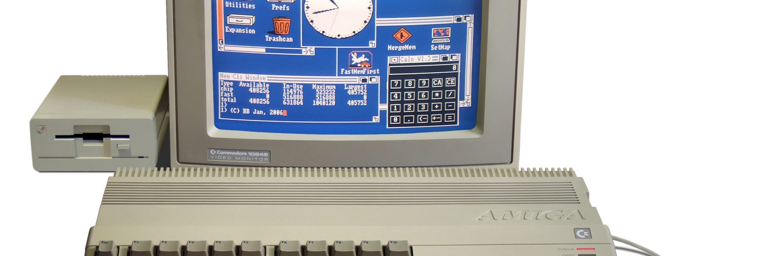
The Amiga Picture above is “© Bill Bertram 2006, CC-BY-2.5 — Attribution. You must give the original author credit.”
You can also use this form below:
Hi Keith,
Love your pages, always a source of inspiration.
Just a “nudge” regarding posting your Cirrus Logic CS4335 DAC Verilog code 🙂
Cheers,
Leslie
Hey!
Thanks for the nudge!
I’ve updated the post to include the entire project directory for Quartus II. This may/may not be relevant to what you’re working on, but be sure to read my updated comment at the bottom of the post for the details.
https://techtravels.org/2016/04/cirrus-logic-cs4335-dac-problems-finally-identified-and-fixed/
Good luck with your project!
Keith
HI Keith,
Thanks a lot for sharing. I would like to know more about MAX 10 UFM accessing. I am planing to write and read UFM using UART interface with an host PC and I don’t want to use NIOS processor for doing that. If you can shed some light on that would be highly appreciated!
Thanks for your comment.
Use the IP Wizard for “Altera On-chip flash” which will launch QSYS. The overall flash storage is broken into two parts: User Flash (for your application) and Configuration Flash (for storing your bitstream to boot the FPGA). This essentially lets you carve up those areas as you see fit.
Be sure that Assignments….Device…Device and Pin options…..Configuration matches what you have configured in that wizard. Otherwise, you’ll get a fatal compilation error.
I forget if there’s an option in the wizard to generate an instantiation template or not, but you’re gonna need one. If you don’t see it in the wizard, right-click the added .qsys file, and generate HDL from there.
The generated UFM controller has an “Avalon-MM” slave bus style interface. Reading from it, you don’t have to do much besides place the address on the bus, and wait (5) clock cycles (the standard latency) for the data to appear on the bus.
I initialize the FLASH with a .MIF file that contains a ROM, so I don’t write to it with Verilog.
There’s a little added complexity with writing because it looks like you have to disable a “write protection” register, you need to hold your write for a specified time, check to ensure that the write was successful, and then re-enable that write protection register. It doesn’t sound hard, but you’ll need some circuitry to handle this. I’d use another FSM.
https://www.altera.com/content/dam/altera-www/global/en_US/pdfs/literature/hb/max-10/ug_m10_ufm.pdf
I’d pay special attention to how the UFM is setup/configured, and then the later diagrams that show the input/output signals, and the read/write timing diagrams. They will tell you essentially everything you need to know.
So setup a top file that instantiates the UARTs, instantiates the UFM, and then use a FSM to control the whole thing.
This should get you started. Feel free to email me keith at this domain if you have follow up questions.