So I bought an FPGA eval board and a book on Verilog awhile back. I made some progress learning things, and had some simple things like UARTs, writing to the LCD, and even some small VGA software(hrrrm, maybe I should call it Hardware…) working. Some of it from scratch, some heavily borrowed from existing sources. But then I got stuck. Stuck on being able to access the DDR on board. The included memory controller, produced by Xilinx’s MIG and the CoreGen app, was hard to use and I didn’t (and still don’t) understand verilog enough to simply run with that controller. Now don’t get me wrong. Xilinx has pretty decent documentation for some of this stuff. And they described pretty well the steps needed to initialize the controller, and perform reads and writes. But you have to remember that their controller is 7300 lines of code broken up across about 40 source files. Now if this was C/C++ or Java (or even assembly language), and it was commented properly, I could probably follow what is being done. Their code is poorly commented IMHO.
I digress, right, but I am really an anal commenter. I comment A LOT. But there really should never be a time where I’ve got explain what’s being done in a particular code block. If something goofy is being done, or if I got sloppy, I explain it in-line with the code. Right on the same line. The comments help me when I’m reading the code. And plus they sometimes reveal bugs in my code where what I say I’m doing in the comments don’t match what’s happening in the code. < digression mode off >
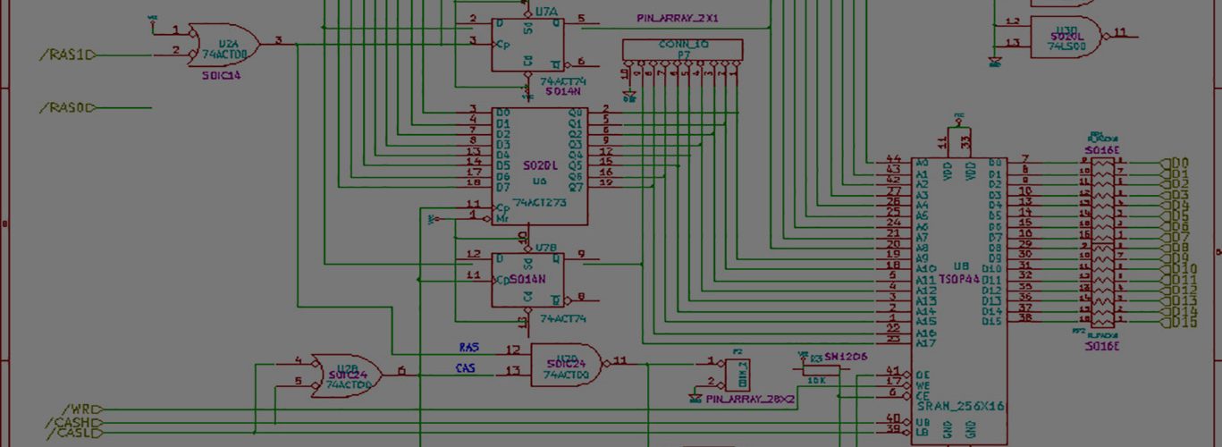
So I’ve been looking for other ways to skin the cat. I’ve asked guys at work. I’ve checked out literally every memory controller on opencores.org. The problem is, basically, that DDR sucks. It first sucks because high frequencies are required and so pathways through the FPGA are restricted. I don’t know enough about FPGAs to tell you which path (from which pin to which pin) meets the timing requirements for DDR. The first D in DDR is double, and that implies that if you have a clock, both the rising edge and falling edge of the clock pulse are reading or writing data. Even if my actual application doesn’t require 100+mhz data rates, I’m forced to read/write to the memory at a fast rate. Oh, and the other D stands for Dynamic. And this sucks too. Why because Dynamic memory has to be refreshed constantly, and on-time. That’s another thing to worry about. And to think I actually contemplated writing my own controller. Sheeeesh.
The Spartan-3 eval board, instead of the 3E (which is what I have), contains 1MB of SRAM. Now the S here is STATIC — aka opposite of Dynamic, no refresh required. It’s fast memory, around 10ns, but it doesn’t do any crap double data rate junk. I’ve seen example controllers for this board, and for this memory, and it’s like one page of code. It’s absurd the difference in complexity. However, I’ve got 64mb, and this is 1mb.
Suffice to say, I don’t own the S3 board. While it’s nice, there are very limited connectors, LED displays instead of LCD, etc
ENTER EDK w/ MICROBLAZE and C
So the embedded design kit, available from Xilinx, contains MicroBlaze which is a 32-bit softcore processor that has BUILT-IN controllers for things like Memory, Ethernet (cool), Serial (UARTs), etc. And guess what, you program it in C. And so you first download the FPGA with the HDL for the softcore, and then you download the .elf executable that is make’d from your code. The Base System Builder (called the BSB) will build some initial framework for you and then you can expand from that. Pretty neat because I can select my exact rev of my starter kit, and it handles many things like making sure that the various chips and onboard peripherals are setup properly and interface to the right pins. So the RS232 port is wired in right, and the ethernet is attached properly. And then, they’ve tested the controllers. To make a long story short, I’ve finally got some code running that accesses the DDR and then spits out some messages via the RS232 port. Now this isn’t my code, but you’ve got to start someplace.
— Entering main() —
Starting MemoryTest for DDR_SDRAM:
Running 32-bit test…PASSED!
Running 16-bit test…PASSED!
Running 8-bit test…PASSED!
— Exiting main() —
So what happens is that the different peripherals are mapped into memory at different locations. On my board, my 64mb of ram is mapped at $8C00 0000-$8FFF FFFF. And how easy is it to read and write to the memory? Check this out:
Defined in an automatically generated header: #define XPAR_DDR_SDRAM_MPMC_BASEADDR 0x8C000000
Xuint32* myram = XPAR_DDR_SDRAM_MPMC_BASEADDR; //declare a pointer to the start of the memory block
myram[0] = 0xAAAA4489;
DONE. That’s it. How much easier can it get!@#
I’m hoping that on Sunday I get some time to spend extending their provided examples. Maybe set up something where it can read in stuff via the serial port, store it in ram, and then spit it back out…
Add comment