So far, I’ve been using a user-selectable mux, with a physical switch, to control which process is connected to the single-port memory controller.
If the switch is in one position, you can upload via USB a properly formatted image. In the other position, the display FSM is active, and it is reading from the memory and displaying it on the output video port.
But since I’m transitioning to a model where I have simultaneous input from the amiga, while outputting to the monitor — things are going to have to get more complicated.
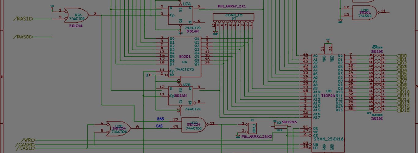
Finding working, easy to use, free memory controllers for FPGAs is tough. A lot of the stuff on OpenCores sucks, and even when they work, there is zero documentation, and reliability is shaky. Sure there are commercial cores.
My memory controller is a freeware wishbone slave. I know I need some type of arbitration, but I’m not even convinced yet that there is enough time (bandwidth?) to allow everyone to properly interleave the access they need. It’s also weird, in that, we read from the memory much faster than we write. Which means that we in essence do unnecessary reads. Do we do some type of per-line synchronization? Can I get away with some other type of scheme?
I’ll take any hints from people who have experience with this stuff.
Important information:
Arriving video information from the amiga comes at a 7.14mhz pixel clock speed, getting 12 bits (16 bits packed) every 140ns. This translates to about 14 megabytes per second. Wow!
Output video is a 25mhz pixel clock, with 12 bits (16 packed) leaving every 40ns. This translates to about 50 megabytes per second.
It’s approximately a 4:1 ratio of reads from memory (aka output to monitor) to writes (aka input from amiga)
My memory is running at 133mhz, and is 16-bit wide. The controller is setup to do a burst size of 2. I think I can access 32 bits every 30ns with a 100mhz user clock best case. So I’m getting at least an effective 1 gigbit / second throughput. This doesn’t include writing it into secondary memory (block ram, etc).
Yeah, I’ve had troubles with this sort of thing myself. The memory controller designs from OpenCores are probably not what you want, since they’re intended to arbitrate between several different customers with unpredictable access patterns. But you’ve got one writer and one reader, both with very regular access patterns. So you’ll probably be best off with some kind of interleaved memory access like you’re contemplating. I assume you’re using SDRAM? That might make things a little more complicated, since you’ve got to fit things into its requirements as well, instead of the totally random access you could get with SRAM.
Can you do something like this:
– Instead of writing directly to memory, have the Amiga write its video data and address to a pair of temp registers, at 7.14MHz. Set a status bit when the registers have valid data.
– Use a 50 MHz memory clock, with alternating A and B memory cycles.
– on A cycles, read 16 bits from the current raster display address, and send it to your display circuit.
– on B cycles, if the input registers hold valid data, then write it to the memory and clear the status bit. Else do nothing.
If you need a larger memory burst size, then your input and output registers could be queues instead.
Yes, SDRAM. I wish it was SRAM.
I don’t have the memory controller really spec’d out to know average/best/worst case times, so that does complicate things…..
Would it be obvious to say that the minimum time for an alternating memory cycle should be the maximum time needed for any one read or write? And then doesn’t longer cycles mean that the time-between-getting-access might be too high?
Just thinking aloud, 20ns isn’t enough time to do a read or a write.
Doing the rough math, there’s enough time to service both the reads and the writes…….
And when you say queues, do you mean a FIFO?
I gotta look at me HDL……
FIFO, yes. Basically you need the *average* write rate to be 16 bits at 7.14 MHz, and *average* read rate to be 16 bits at 25 MHz. But you can use some registers or a small FIFO on either the read or write end (or both), to support a more bursty I/O. For example, you could read out an entire line of video in one transaction, then use the memory for writes the rest of the time until a new video line begins. And use a FIFO to save any writes that occur while the video line read is happening.
I am very much chewing on these comments right now. I currently do process the reads from DRAM to ALTRAM based on trigger of the horizontal address = 0. My hope, of course, is that the read wouldn’t take longer than the front porch & other stuff that happens before the video signal needs to be active.
Before I wrote any code, I’ve been trying to determine exactly how long a read takes, and how long a write takes….
I originally thought that this WAS taking less time, because it was working, so I’m really not sure what’s going on yet.
Lots of experimentation and logic analyzer time.