As you may have seen in this other post here I have an interest in this Amiga hard drive controller designed for the Commodore Amiga 500. I used this for years to interface an HDD. At the time I took some photos of the PCB and shared some my notes, I also dumped the Boot ROM from the board, which had already been done previously — and compared it. I did it both as an exercise to play with this stuff, but also to see if mine differed from existing sources, which it did not.
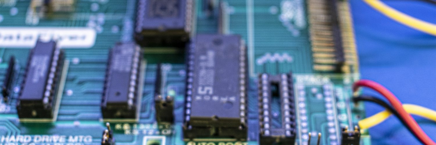
The rest of the board has fairly off-the-shelf 74 logic chips which are called out in that other post, along with the main chip being the AM5380 SCSI IC on the PCB.
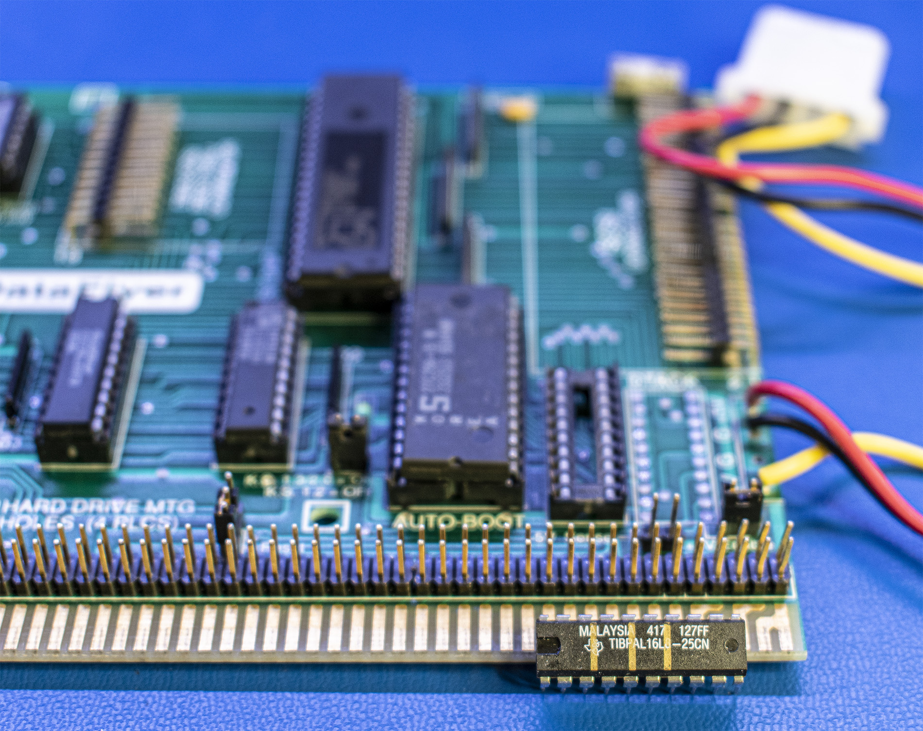
One piece of engineering, though, that I assume is custom to Expansion Systems was their PAL. I don’t know what its main function is, but I’m starting to collect information to the form the picture. When these type of chips die, you don’t just go on digikey or mouser and get a new one. So understanding how they work and “backing up” what they do precisely helps preserve these things for the future.
These notes are raw and unrefined, but Bob reminded me that there’s very little specific information about this PAL anywhere on the internet, and thought I’d share.
This exercise was important to determine how the inputs and outputs are being used to determine the optimal dumping strategy.
Pin connections for the TIBPAL16L8-25CN labeled BUSS on the DataFlyer 500 SCSI-only version.
Pins 1-9, and 11 are input-only on the PAL
Inputs: The PAL makes decisions on how to set the output pins based on the following criteria
Pin 1: This is high if Amiga Address bus A1 or A2 is high
Pin 2: This is low if the comparator match is valid, and the Amiga asserts address strobe. Probably an active_low enable signal for the board.
Amiga card edge connections
Pin 3 – 6: Amiga outputs address bus A3, A4, A5, A6 to these pins, plus feeds ROM A2, A3, A4, A5
Pin 7: Amiga outputs R_W signal. High for Reads, Low for Writes.
Pin 8: Amiga outputs A15
Pin 9: Amiga outputs _UDS. Upper Data Strobe
Pin 11: RESET. Controlled by PCB jumper or Amiga output, which asserts during a reboot.
Pin 13: This PAL I/O pins appears to be used as a INPUT. Driven by Amiga _CCK clock.
Pin 18: 373 Output Enable. Also DTACK pin 3. And pin 12 header, jumpered to card edge 11. This is driven by the Amiga _CONFIG.
Outputs: The PAL outputs these signals to be consumed by other devices.
Pin 12: ROM Chip Enable. Also pin 1 on 244.
Pin 14: 373 Latch Enable.
SCSI 5380 connections
Pin 15: _IOR. I/O READ. Used to read an internal register selected by _CS and A0-A2. It also selects the Output Data Register when used with _DACK.
Pin 16: _IOW. I/O WRITE. Used to write an internal register selected by _CS and A0-A2. Also selects Output Data Register when used with _DACK.
Pin 17: _DACK. DATA ACKNOWLEDGE. Resets DRQ (DMA Request) and selects the data register for input or output data transfers.
Pin 19: _CS. CHIP SELECT. Enables a read or write of the internal register selected by A0-A2
More details
The 8-bit comparator compares the Amiga address bus A23 to A16 with the output from the 373 latch.
The latch gets its values from the Amiga data bus, D15 to D8.
The latch enable is an output from the PAL pin 14.
Disclaimer: This is a work in progress, and info is changing rapidly. Make sure to refresh your cache!
Status: A “real” schematic is coming soon which will reduce the need for posts like this.
You wouldn’t happen to have a dump of the DFI PAL, or a file to re-produce the chip do you? The chip in my DataFlyer is bad.
Which version do you have? Scsi, ide, or both?
On PALs like this you can’t easily dump them. I’ve just started reverse engineering that one. Got another couple projects on the side that are taking precedence.
I expect to make some progress on it within the next month or so. So check back. Not all versions I think are the same, so let me know.