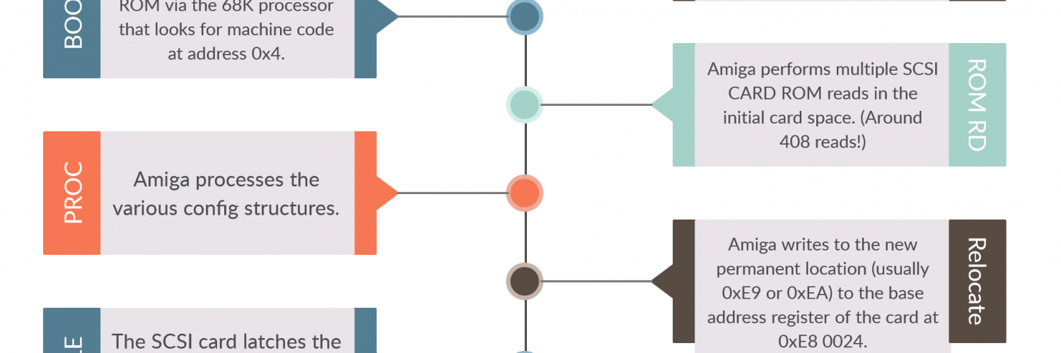

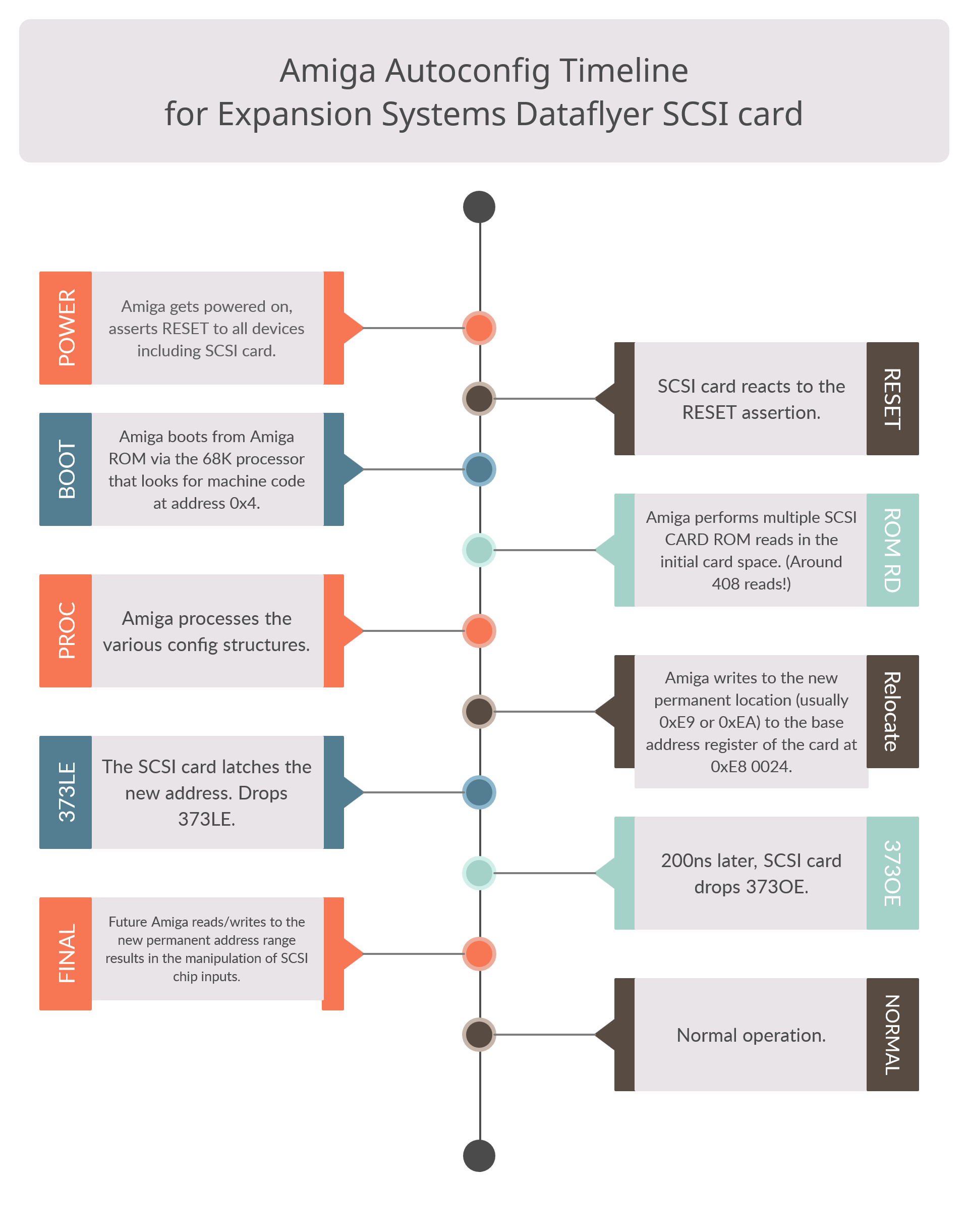
It’s often useful when trying to understand, debug, or reverse engineer a system to put together a timeline of operation from beginning to end. The result is a series of events where something happens first, then something else, perhaps some more “middle steps”, and finally the last thing. This can yield definitions of overall phases, states, and perhaps transitions from one state to the next. Wrapping our heads around these ideas will help educate us on what state the PAL is responsible for maintaining, if any.
Let’s apply this idea to our example. In our example of reversing the SCSI PAL which sits on a card which interfaces to the Commodore Amiga, you’ll want to look from the perspective of the Amiga, from the whole system level because that’s who’s running the show.
To state or not to state, that is the question….
John D Barrow
I was assembling a state diagram for this blog post, but decided against doing so. Part of it is admittedly laziness, but there’s a much more important reason: simply not implying a state machine design, where none exists. As the overall theme of this blog series promotes, understanding the overall context in which your PAL finds itself is important. As a result, you should investigate the various states that your PAL will find itself in. Establishing a timeline of activity helps give you delineation of function, and will help decompose the problem into smaller functional chunks which you can use as milestones as you attempt to duplicate the PAL.
However, you should realize that there’s a difference between simply logically grouping time-correlated outputs and the PAL necessarily utilizing any programming construct to operate like a state machine. While PALs can support finite state machines directly, some significant portion(I hesitate to say most, because I really don’t know this) of PAL designs have completely independent output pins which should get separate attention. There’s no need to bundle them together and doing so will over complicate your task.
For many designs, then, each output pin is simply the boolean algebraic evaluation of the associated equation, without awareness of any other output pin, or the overall state of the system.
Keith, 2022.
While two output pins may have a logical mutual exclusion, for instance, the PAL doesn’t know this, and doesn’t enforce this in any way. For example, with this SCSI card, the PAL has to output a READ pin and a WRITE pin for the 5380 SCSI chip. They both can’t be low at the same time, but the PAL doesn’t care. If the equation for the read output is true, and the equation for the write output is true, then that’s the states those pins will take. Regardless of the inevitable failure that looms. 🙂
Please realize that while I’m trying to promote increasing your conceptual awareness of the system by examining states, that there’s a big difference between CONCEPT and IMPLEMENTATION.
So if you group these events you get essentially 5 states from the perspective of the SCSI card:
- Pre-latch IDLE: All outputs are a 1. This is the default state, and also the state that the card goes into when RESET is asserted.
- Pre-latch ROM read: Handle the inbound SCSI CARD ROM reads, ROM CE is a 0, everything else is a 1.
- Post-latch IDLE: All outputs, except for 373LE(now 0-bit), have a value of 1. Card is now sitting at the new address.
- Post-latch IDLE OE: All outputs, except for 373LE and 373OE (both 0-bit), have a value of 1.
- Post-latch R/W events: Based on reads writes to the new address range, toggle the SCSI chip inputs as appropriate.
The bulk of the time the card sits in the “Post-latch IDLE OE” state, unless an active read/write is occurring.
You’ll want to understand the various transition events that cause your device to move from state to state:
If the RESET pin is asserted, go to pre-latch IDLE.
If a ROM read occurs, go to pre-latch ROM READ, until the read is over.
If a write to the base address register occurs, go to “Post-latch IDLE” temporarily.
Upon completion of the base address register write, go to “Post-latch IDLE OE”
If a read/write occurs after the latch event, handle the post-latch R/W event.
Add comment