Note that this page is no longer being updated, please see github link below!
https://github.com/KS10FPGA/KS10FPGA
The Digital Equipment Corporation (DEC) KS10 was a low cost implementation of the popular PDP-10 mainframe computer. I’ve always wanted my on PDP-10 and now I’ve decided to build my own. How hard could that be?
The goal of this project is to re-implement the DEC KS10 using modern components and technology. This project retains microcode compatibility with the original DEC KS10 in order to maximize the probability that this design will behave exactly like the original DEC KS10 implementation.
The entire KS10 Central Processing Unit (CPU) is implemented in a single Field Programmable Gate Array (FPGA) instead using of boards of discrete logic. The FPGA is firmware is written in Verilog and currently consists of about 33,000 lines of code plus comments. Similarly, the Console Processor is implemented in a single-chip ARM Cortex M3 microcontroller whereas the DEC KS10 used an Intel 8080 microprocessor and a board full of logic. The console software is written in a mixture of C and C++ and is about 20,000 lines of code plus comments (excluding the lwIP TCP/IP stack).
The KS10 FPGA peripherals are significantly different than the legacy DEC KS10 peripherals. Modern peripherals like Secure Digital High-Capacity (SDHC) solid-state disk drives replace the Moving Head RP06 disk drives and TU45 9-track magtape drives. Even though the physical devices are different, the original hardware interfaces have been retained. The disk drives use the same bits-on-disk formatting as the SIMH simulator so that files (and disk images) may be moved between SIMH and the target hardware without modification. Universal Serial Bus (USB) and Ethernet devices are provided in addition to standard legacy RS-232 devices.
The KS10 FPGA is currently implemented using a 12.5 MHz clock. At this speed, the KS10 FPGA is on-average 4x faster than the DEC KS10. I believe that it will be easy to increase the clock speed by another 2x to 4x when the design is stable. A sumary of the instruction timing of the two machines is available in this report.
Contents
News (Last Updated on 09 May 2016):
The KS10 FPGA software and firmware is now available at https://github.com/KS10FPGA/KS10FPGA. Go visit the Github page.
Things I’m working On
- The Pager is still broken. I’ve kludged in more changes but it is clearly not still correct. I have created a short paper (available here) that describes the correct operation the KS10 Pager. It also describes what is broken any why.
- I’ve hacked the KS10 Console to create some page table entries in KS10 memory, enable paging, load the various diagnostics into KS10 memory from an SD Card, and then execute the diagnostic. Now I can execute the Basic and Advanced Instruction Diagnostics with paging enabled. More importantly I can do this from the Verilog Simulator and see what is happening.
- I’ve hacked-up a special version of the Pager which can be conditionally compiled into the design. Normally the Pager handles the page translation for a whole page of addresses which only exposes Pager issues on page boundaries. This specially hacked-up Pager remembers the entire Virtual Memory Address (VMA) associated with the page fill. When a memory access occurs, this Pager will provide the correct page translation only when the VMA that is presented is exactly the same as the page fill. It will generate a page failure for every other VMA. This guarantees that every new memory access will generate a page failure. This just hammers the paging hardware and exposes issues quickly.
- When I try to boot TOPS-10, the KS10 FPGA prints the Monitor Pre-boot Banner and then crashes as follows:
KS10> BT
BOOT V3(47)
The next goal is to get it to execute to the BOOT> prompt.
Recent Accomplishments
- I have added a Hardware Breakpoint facility to the KS10. The Breakpoint Facility can match instruction fetches, memory reads and writes, and IO reads and writes.
- I have also added an Instruction Trace Buffer facility. The Trace Buffer captures the Program Counter and the Instruction Register.
- The Pager was redesigned. The FPGA synthesis tool originally built the Pager Address Translation Memory out of 8130 flip-flops. The FPGA has various kinds of “Block Memory” on-chip but I could not coax the the synthesis tool to infer the right kind of memory. Worse yet, the the DEC KS10 Pager employed two interleaved memories so that the microcode could invalidate two entries at a time – as a speed optimization. I finally instantiated a strange Xilinx Dual Port Memory where the two ports have different aspect ratios: the write port is two entries wide and appears as a 256×36 bit memory while the read port is one entry wide and appears as a 512×18 bit memory. The wide write port allows the two-at-a-time page invalidation while the narrow read port does not require a multiplexer (which was a speed problem) to select between two interleaved memories. The FPGA resource utilization dropped by twenty percent. Problem solved.
- I have uploaded the KS10 FPGA Processor Manual (Rev 40).
Processor Manual and Documentation
Most of the really interesting details of the KS10 FPGA design is documented in the
KS10 FPGA Processor Manual (Rev 40). This is a working document which provides the rationale for much of the design details. It also provides a detailed description on the KS10 CPU and Peripherals gleaned from the various documents and diagnostic software.
I’ve uploaded a paper that describes the process or debugging the KS10 Priority Interrupt system within the context of the Verilog Simulator. If you’re curious what debugging the FPGA looks like, the paper is available at the following link: KS10 Interrupts.
I’ve uploaded another paper that describes the process of verifying the KS10 CPU in the target FPGA hardware using the Xilinx ChipScope embedded logic analyzer. The paper is available from the following link: KS10 FPGA CPU Debugging with Xilinx ChipScope.
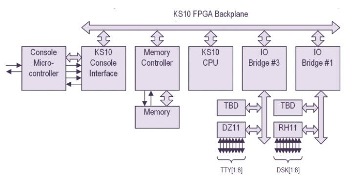
KS10 FPGA System Diagram
The KS10 FPGA consists of the KS10 CPU, Memory Subsystem, Console Subsystem, and a pair of IO Bus Bridges. An DZ-11 8-Port Terminal Multiplexer is implemented on one IO Bus and an RH-11 Massbus Controller with 8 RP06 Disk Drives is implemented on the other IO Bus.
The block diagram is illustrated below:
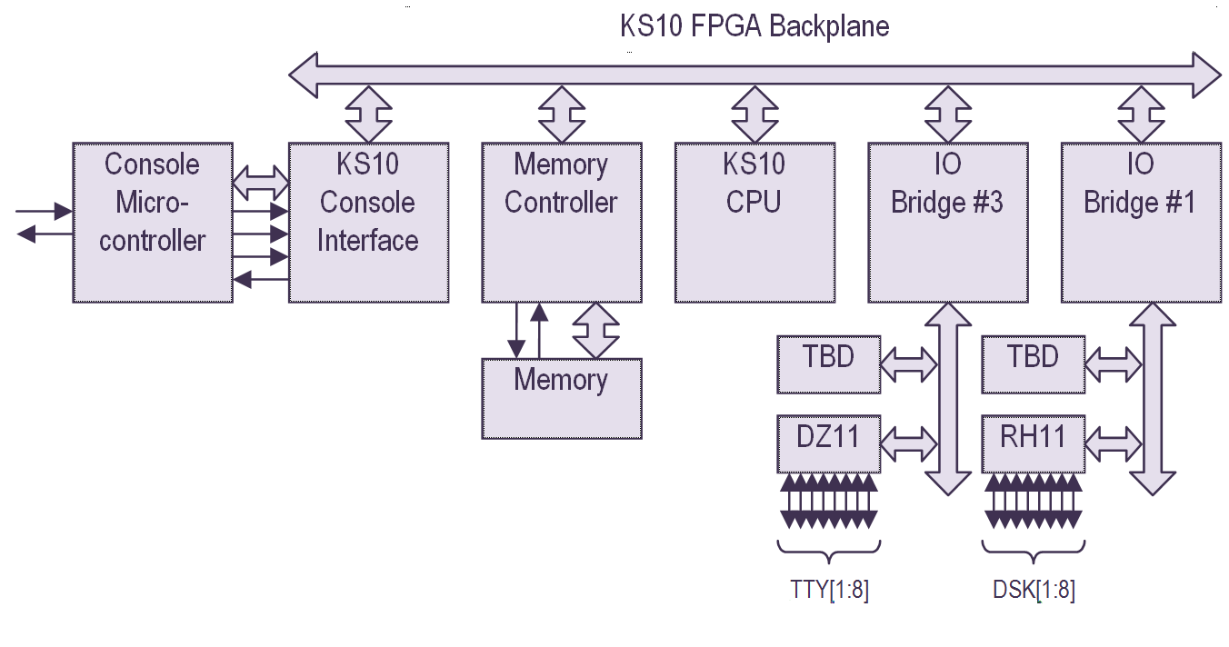
The status of each of these large blocks of functionality illustrated above is summarized in the following sections.
General Status:
KS10 CPU
The CPU design is very stable. Although the Pager works properly in the simulation, the Pager is problematic in the target hardware and I suspect that this is because of a significant design problem.
The diagnostic status of the KS10 CPU is summarized below:
DSKAAA0 DECSYSTEM 2020 BASIC INSTRUCTION DIAGNOSTIC ( 1) . . . . Pass   Pass
DSKABA0 DECSYSTEM 2020 BASIC INSTRUCTION DIAGNOSTIC ( 2) . . . . Pass   Pass
DSKACA0 DECSYSTEM 2020 BASIC INSTRUCTION DIAGNOSTIC ( 3) . . . . Pass   Pass
DSKADA0 DECSYSTEM 2020 BASIC INSTRUCTION DIAGNOSTIC ( 4) . . . . Pass   Pass
DSKAEA0 DECSYSTEM 2020 BASIC INSTRUCTION DIAGNOSTIC ( 5) . . . . Pass   Pass
DSKAFA0 DECSYSTEM 2020 BASIC INSTRUCTION DIAGNOSTIC ( 6) . . . . Pass   Pass
DSKAGA0 DECSYSTEM 2020 BASIC INSTRUCTION DIAGNOSTIC ( 7) . . . . Pass   Pass
DSKAHA0 DECSYSTEM 2020 BASIC INSTRUCTION DIAGNOSTIC ( 8) . . . . Pass   Pass
DSKAIA0 DECSYSTEM 2020 BASIC INSTRUCTION DIAGNOSTIC ( 9) . . . . Pass   Pass
DSKAJA0 DECSYSTEM 2020 BASIC INSTRUCTION DIAGNOSTIC (10) . . . . Pass   Pass
DSKAKA0 DECSYSTEM 2020 BASIC INSTRUCTION DIAGNOSTIC (11) . . . . Pass   Pass
DSKALA0 DECSYSTEM 2020 BASIC INSTRUCTION DIAGNOSTIC (12) . . . . Pass   Pass
DSKAMA0 DECSYSTEM 2020 BASIC INSTRUCTION DIAGNOSTIC (13) . . . . Pass   Pass
DSKBAA0 DECSYSTEM 2020 BASIC INSTRUCTION RELIABILITY DIAGNOSTIC  Fail   Pass
DSKCAA0 DECSYSTEM 2020 ADVANCED INSTRUCTION DIAGNOSTIC (1) . . . Pass   Pass
DSKCBA0 DECSYSTEM 2020 ADVANCED INSTRUCTION DIAGNOSTIC (2) . . . Pass   Pass
DSKCCA0 DECSYSTEM 2020 ADVANCED INSTRUCTION DIAGNOSTIC (3) . . . Pass   Pass
DSKCDA0 DECSYSTEM 2020 ADVANCED INSTRUCTION DIAGNOSTIC (4) . . . Pass   Pass
DSKCEA0 DECSYSTEM 2020 ADVANCED INSTRUCTION DIAGNOSTIC (5) . . . Pass   Pass
DSKCFC0 DECSYSTEM 2020 ADVANCED INSTRUCTION DIAGNOSTIC (6) . . . Pass   Pass
DSKCGB0 DECSYSTEM 2020 ADVANCED INSTRUCTION DIAGNOSTIC (7) . . . Fail   Fail
DSKDAB0 DECSYSTEM 2020 CPU AND MEMORY RELIABILITY DIAGNOSTIC . . Fail   Fail
DSKEAA0 DECSYSTEM 2020 PAGING HARDWARE DIAGNOSTIC  . . . . . . . Pass   Fail
DSKEBA0 KS10 - CACHE DIAGNOSTIC  . . . . . . . . . . . . . . . . Fail   Fail
DSKECB0 KS10 - KL-PAGING DIAGNOSTIC  . . . . . . . . . . . . . . Fail   Fail
DSKFAA0 DECSYSTEM 2020 INSTRUCTION TIMING DIAGNOSTIC . . . . . . Fail   Pass
* Passes relevant tests with paging disabled.
I have added a Hardware Breakpoint facility to the KS10. The Console can set breakpoints on Instruction Fetches, Memory Reads, Memory Writes, IO Reads, and IO Writes. When a breakpoint occurs, the KS10 generates a “Console Halt”. I may go back and add a supervisor level interface like the DEC KL10 – but that would require microcode changes. I’m not prepared to spend that much time on it right now.
I also added an instruction trace facility. Now I can capture instruction traces and dump the trace from the console. The Trace Buffer captures the Program Counter (PC) and the Instruction Register (IR).
Memory Controller
The evaluation board includes a single Cypress Semiconductor CY7C1460AV33 1 MW x 36 Synchronous Static RAM (SSRAM) memory device. SSRAM was chosen for the first implementation because it is a single chip, is very fast (166 MHz) which eliminate the need for the cache, and provides a simple interface to the FPGA. Cypress Semiconductor also provides a very accurate simulation model which has been incorporated into the testbench.
Why provide 1 MW of memory when the KS10 was limited to 512 KW of memory? It is common folklore that the KS10 was architecturally limited to 512 KW of memory. This is not true. This was either a memory technology limitation or a marketing limitation but was not an architectural limitation. The KS10 had 8 memory cards slots and each DEC memory card provided maximum of 64 MW of memory – for a total of 512 KW of memory. The KS10 internal memory address paths have always supported 20-bit addressing. For example ADP Onsite resold modified DEC KS10s with 1 MW of memory. An example of a KS10 that had 1 MW of memory can be seen at the Rhode Island Computer Museum.
Because the SSRAM memory has a 2 stage pipeline, the memory controller and SSRAM operates at four times the CPU clock rate. This hides the memory pipeline from the CPU and creates the illusion that memory reads and memory writes complete in a single CPU clock cycle.
The diagnostic status of the KS10 memory controller (and memory) is summarized below:
                           DIAGNOSTIC                            SIM   TARGET
---------------------------------------------------------------- ----   ----
DSMMAB0 DECSYSTEM 2020 KS10 1024K MEM DIAG . . . . . . . . . . . Fail*   Pass
DSMMBA0 DECSYSTEM 2020 BLT/FLOATING 1-0 MEMORY EXERCISER TEST  . Fail*   Pass
DSMMCB0 DECSYSTEM 2020 FAST AC DIAGNOSTIC  . . . . . . . . . . . Fail*   Pass
DSMMDC0 DECSYSTEM 2020 MEM DIAG  . . . . . . . . . . . . . . . . Fail*   Pass
* I obviously haven’t set up the simulator properly to run these diagnostics.
“Unibus” IO Bus Bridge
The IO Bus Bridge interfaces the peripherals on the IO bus to the KS10 backplane bus. The original DEC KS10 used 16-bit/18-bit Unibus-based peripherals while the KS10 FPGA uses a 36-bit synchronous IO bus that is better suited to an FPGA implementation. The KS10 FPGA IO Bus also uses significantly fewer clock cycles to implement the IO bus protocol.
The KS10 could address up to four Unibus Bridges although only two were commonly supported. The IO Bus Bridge is fully parameterized so all of these configurations are supported by the UBA module. The KS10 FPGA currently provides UBA1 supporting the RH11 Massbus Disk Controller and UBA3 supporting the DZ11 8-port Terminal Multiplexer.
The IO Bus Bridge provides paging (Virtual Address/Physical Address translation) for the peripherals and a Status Register. The KS10 FPGA does not implement the (mostly undocumented) Maintenance Loopback Mode.
The diagnostic status of the KS10 IO Bus Bridge (both devices) is summarized below:
                           DIAGNOSTIC                            SIM   TARGET
---------------------------------------------------------------- ----   ----
DSUBAC0 DECSYSTEM 2020 UNIBUS ADAPTER EXERCISER  . . . . . . . . Pass   Pass*
* Includes expected failures because the Maintenance Loopback Mode is not implemented. The Maintenance Loopback Mode is only used by the diagnostic program and is not required for any of the Monitor programs.
DZ11 8-port Terminal Multiplexer
The DZ11 is an asynchronous multiplexer that provides an interface between the KS10 processor and eight asynchronous serial ports. It provides a means to control baud rate, character length, number of stop bits, parity, and transmitter/receiver interrupts for each of the eight serial ports. Lastly, the DZ11 provides some FIFO buffering (DEC called it a SILO) so that the KS10 processor did not need to service the DZ11 on every character that was received.
A block diagram of the DZ11 interface is illustrated below.
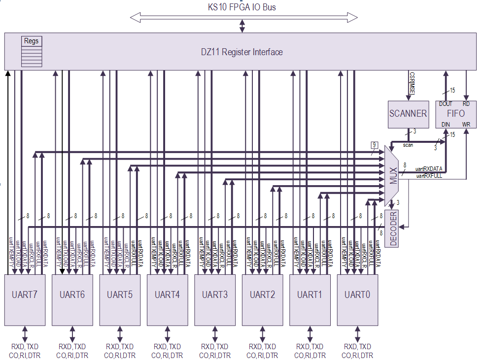
The DZ11 module is fully parameterized for IO Base Address, Interrupt Number, Interrupt Vector, and supports the four device configuration that are documented in the Appendix B.3 of the KS10 Technical Manual. The KS10 FPGA currently is only configured for the DZ11 at the 3760010 IO Base Address.
Although the DZ11 supports 8 serial interface, the KS10 FPGA evaluation board only provides two TTY interfaces. The other six TTY interfaces are tied-off internally.
I have been thinking more and more about providing an alternate DZ11 design that routes the 8 TTY ports through an Ethernet interface. The DZ11 has a FIFO for the receive data which would make a clean interface between a telnet-like daemon in the console and the remainder of the DZ11 hardware. Something similar could be implemented for the transmit data.
The DZ11 Technical Manual is available from bitsavers.org
The diagnostic status of the DZ11 Terminal Multiplexer is summarized below:
                           DIAGNOSTIC                            SIM   TARGET
---------------------------------------------------------------- ----   ----
DSDZAB0 DECSYSTEM 2020 DZ11 ASYNC L MUX  . . . . . . . . . . . . Pass   Pass**
* The DSDZA diagnostic needs patched to in order to work correctly with the KS10 FPGA. The DSDZA diagnostic uses instruction-based timing loops for timeouts and these timeout need to be modified (increased significantly) to work with the faster FPGA implementation. Fortunately the delay count is tabularized with one entry for each baud rate. This table is called “DLYTBL:” and is at location 035650.
RH11 Massbus Disk Controller
The KS10 FPGA includes an a Disk Controller that is register compatible with the RH11 Massbus Disk Controller. This disk controller ‘front-ends’ a single Secure Digital High-Capacity (SDHC) disk card interface that emulates an array of 8 RP06 Disk Drives.
A block diagram of the RH11 Disk Controller and the RP06 Disk Drive emulator is illustrated below.
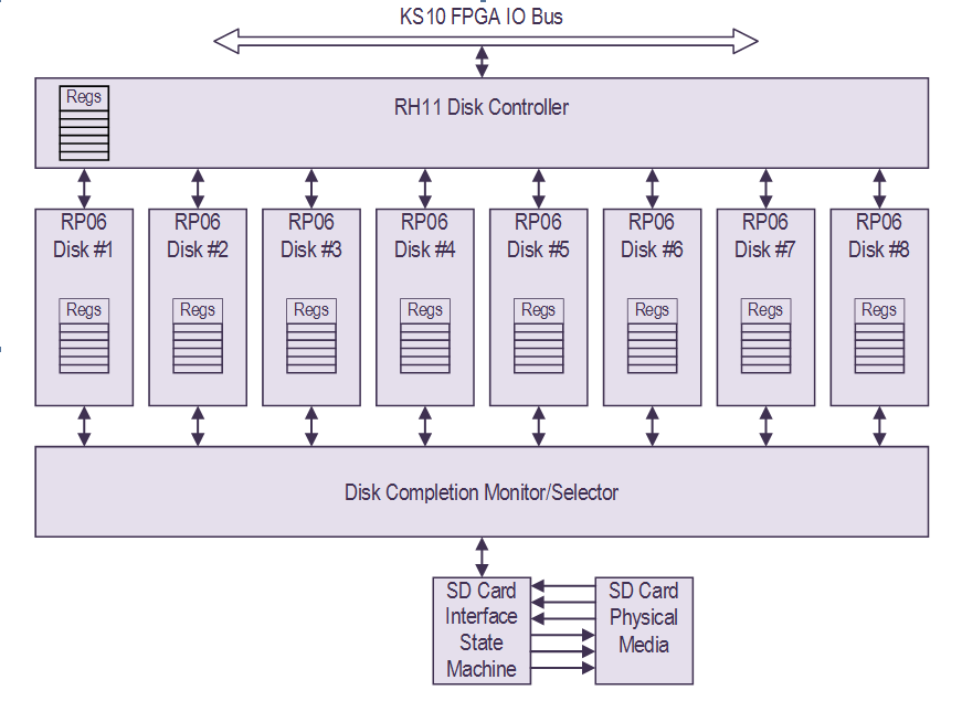
Unlike some of the other KS10 circuitry, the RH11 controller in the KS10 FPGA deviates significantly from the DEC RH11 design. The design uses modern inexpensive solid state Secure Digital High Capacity (SDHC) media for the disk drives. The design is fully parameterized to support the implementation of varying sized (and geometry) of disk drives. It can be conditionally compiled to support the the following disk drive types:
- RP04
- RP05
- RP06
- RP07
- RM03
- RM05
- RM80
Having said that, only the RP06 has received any testing at all. The RMxx series disks may require a little tweaking. Lastly I don’t have any good diagnostics for the other disk drives.
The RH11 Massbus Controller and RP06 Disk array appears to be working. I built an RP06 Reliability Exerciser and Diagnostic Pack (RED Pack) from the tape image in SIMH and copied the disk image to the Secure Digital (SDHC) Card. To my complete surprise, I can actually navigate around the Tops-20 RP06 Red Pack disk and successfully execute many of the tests successfully. The RED Pack was used to “demonstrate to the customer, the forty-eight hour Hardware Reliability portion of System Acceptance” – so it is a very useful hardware debugging aid. A transcript from the TTY has been captured in the document entitled Exploring the REDPACK.pdf.
The diagnostic status of the RH11 and RP06 is summarized below:
                           DIAGNOSTIC                            SIM   TARGET
---------------------------------------------------------------- ----   ----
DSRPAC0 DECSYSTEM 2020 KS10/RH11 - RP06 BASIC DEVICE DIAGNOSTIC  Pass   Pass*
DSRMB0  DECSYSTEM 2020 RH11 - RM03/RP06 - RELIABILITY DIAGNOSTIC ????   ????*
* Includes expected failures because the RP06 Diagnostic Mode is not implemented. The RP06 Diagnostic Mode is only used by the diagnostic program and is not required for any of the Monitor programs.
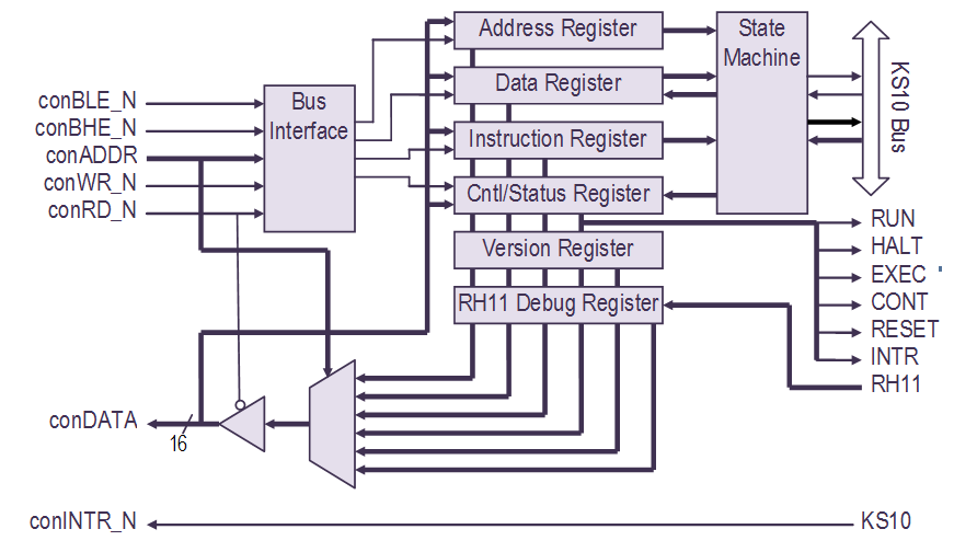
Console
Unlike modern computers, the KS10 can’t actually bootstrap itself without support from the Console Microcontroller. Early PDP10 computers required the operator to key in the bootstrap program from the front panel interface using switches and lights. The DEC KS10 simplified the boot processes when it employed an Intel 8080 microprocessor and a board full of support circuitry to perform this function.
Like the DEC KS10 implementation, the KS10 FPGA appears as a Memory Mapped IO device of the Console Microcontroller. The Console Microcontroller controls how the firmware is loaded into the FPGA, loads the KS10 executables into memory, and starts the KS10 processor. Once the KS10 FPGA is operating, the Console Microcontroller provides the CTY interface. The KS10 executable can be either one of the diagnostic programs or the monitor program.
A block diagram of the console register interface in the KS10 FPGA is illustrated below.
Console Hardware
The Console Microcontroller is implemented almost entirely by a Texas Instruments/Stellaris LM3S9B96 (ARM Cortex-M3) single-chip microcontroller. This microcontroller operates at 50 MHz and includes:
- 256 KB Flash memory
- 96 KB SRAM
- External Peripheral Interface (EPI). The KS10 FPGA interface is memory mapped using the EPI interface.
- 3x Universal Asynchronous Receivers/Transmitters (UARTs). These are used for serial communication
- Synchronous Serial Interface (SSI). The Secure Digital (SD) Card interface uses the SSI interface.
- Ethernet controller.
- Universal Serial Bus (USB) controller. The USB interface is currently unused.
- ROM Containing:
- Stellaris Boot Loader and vector table
- Stellaris Peripheral Driver Library (DriverLib) release for product-specific peripherals and interfaces
- SafeRTOS code
- Advanced Encryption Standard (AES) cryptography tables
- Cyclic Redundancy Check (CRC) error detection functionality
Console Software
The console software is an application built on top of the SafeRTOS Real Time Operating System (RTOS) for embedded processors. SafeRTOS provides rudimentary priority-based multitasking, queue-based intertask communications, semaphores, other simple OS features. More interestingly, the SafeRTOS executable is built-in to the Console Microcontroller’s ROM – so it doesn’t use any Flash Memory.
The console software uses a mix of off-the-shelf and custom software components. The off-the-shelf software components that are used by the console software are listed below:
- Revision 9107 of the Stellaris Peripheral Driver Library – Copyright (c) 2005-2012 Texas Instruments Incorporated. This library is located in the internal ROM of the LM3S9B96 microcontroller.
- SafeRTOS – Copyright (C) Wittenstein High Integrity Systems. The SafeRTOS object code is also located in the internal ROM of the LM3S9B96 microcontroller.
- FatFs R0.09b – FAT Filesystem – Copyright (C) 2013, ChaN, all right reserved.
- lwIP TCP/IP stack – Copyright (c) 2001-2004 Swedish Institute of Computer Science.
The Console Microcontroller is implemented using a mix of C and C++ software – most of the KS10 console software is implemented in C++ while the COTS FAT32 filesystem software and the TCP/IP stack is implemented in plain old C. All code is built using a GCC embedded ARM toolset. All the software interacts directly with the hardware – there is no operating system to provide support services. The code can be loaded into the LM3S9B96 microcontroller using the openocd application via the USB hardware that is included on the board.
Console Operation
The console software initializes the microcontroller, performs a few self-tests on the hardware, loads the Xilinx FPGA with firmware, displays the contents of the KS10 FPGA Firmware Revision Register, initializes the SD Card device, and mounts a FAT32 filesystem on the SD Card device.
Once that is all completed, the Console Microcontroller un-resets the KS10 FPGA and the KS10 FPGA begins executing microcode. The KS10 microcode initializes the Arithmetic Logic Unit (ALU) registers, initializes variables stored in the RAMFILE, and performs a basic built-in test of the ALU. Once this is completed, the KS10 FPGA microcode halts and waits for the Console Microcontroller to load some boot software into the KS10 memory. The console software detects that the KS10 FPGA has halted, correctly recognizes that reason for the halt, and prints the “Halt Status Block” on the console terminal.
The console is configured for 9600 baud, no parity, 8 data bits, 1 stop bit.
The console boot sequence is as follows (subject to change…):
CPU : Console alive.
CPU : Device identifier is 0x10040203.
NET : MAC Address is 01:1a:b6:00:64:00
NET : Successfully started telnet task.
NET : Telnet servers started.
CPU : EPI interface initialized.
KS10: Programming with firmware. . . . . . . .
KS10: Programmed successfully.
KS10: Firmware is REV 00.10
KS10: Console Interface Register test completed successfully.
SDHC: Card inserted.
SDHC: SDHC Card Initialized Succesfully.
SDHC: FAT filesystem successfully mounted on SD media.
KS10: Halted.
KS10: Halt Cause: Microcode Startup. (PC=000000)
  Halt Status Block Address is 376000
  PC  is 000000000000     HR  is 702300000100
  MAG is 377777777777     ONE is 000000000001
  AR  is 000000000100     ARX is 000000000001
  BR  is 000000376000     BRX is 000373000420
  EBR is 000000000000     UBR is 000000000000
  MSK is 777777777777     FLG is 000000000000
  PI  is 000000000000     X1  is 000001000001
  TO  is 000000000000     T1  is 000000000002
  VMA is 140000000000
KS10: RH11 successfully initialized SDHC media.
KS10>
At this point, the operator can do several things. He can:
- Load a KS10 program from the SD Card.
- Load the SMMON Diagnostic Monitor from the SD Card. This might be useful if all of the RP06 disk drives are damaged.
- Load the SMMON Diagnostic Monitor from one of the RP06 disk drives.
- Load one of the operating systems (Monitors) from one of the RP06 disk drives.
Console Status
Right now the Console Microcontroller’s software functionality is still very basic. Software is being added as required to debug the KS10 FPGA firmware and hardware.
The diagnostic status of the KS10 Console is summarized below:
                           DIAGNOSTIC                            SIM   TARGET
---------------------------------------------------------------- ----   ----
DSLTA   DECSYSTEM 2020 TELETYPE TEST . . . . . . . . . . . . . . ????   Pass
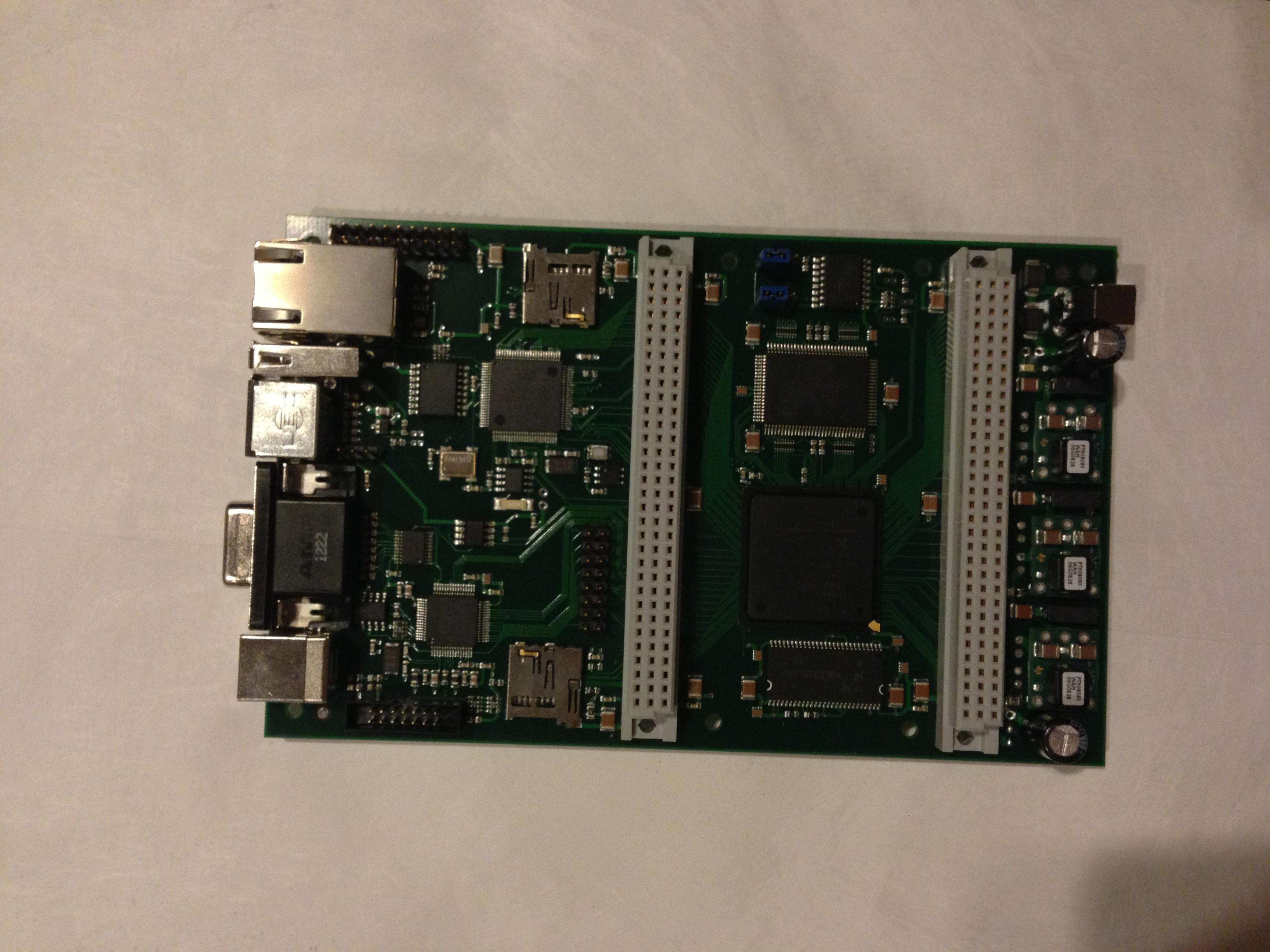
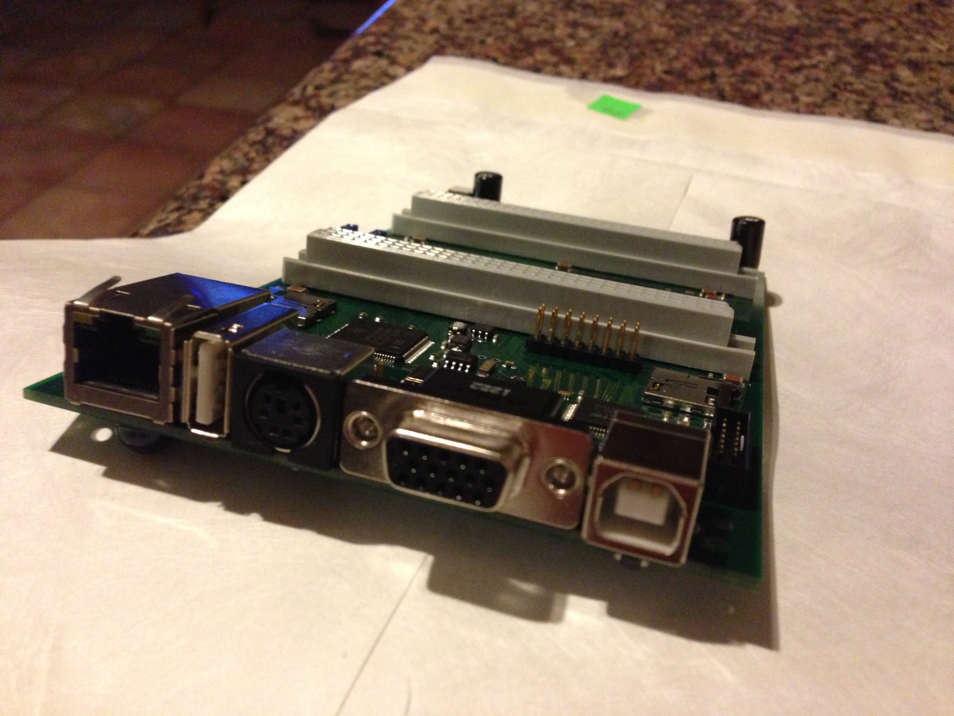
The ESM-BB10 KS10 FPGA Board
A KS10 FPGA prototype circuit card was designed and built by Emanuel Stiebler. In correspondence, he calls it the ESM-BB10 – so I’ll use his terminology. The design and workmanship appears to be top-notch — it’s just plain beautiful.
The ESM-BB10 circuit card features:
- Xilinx Spartan 6 XC6SLX45-2-FGG676 FPGA
- 1 MW x 36 SSRAM (166 MHz)
- 32MW x 16 SDRAM (133MHz)
- 4 Serial Ports (TTY/CTY) ‘tunneled’ through USB
- Micro SD Card Slot for 8x RPxx Disk Drives
- PS/2 Keyboard and Mouse Interfaces
- VGA Interface
- Real Time Clock
- ARM Processor with 10/100BASE-T Ethernet, Micro SD Card Slot, and USB interface
Because Emanuel added Ethernet to the Console, I think we’re going to have to figure out how to add networking to the KS10. After all, we have a co-processor to handle all the nasty little details.
Some photos of the prototype hardware:
(You may click on the image for an enlarged version).
It turns out that the off-the-shelf FPGA boards are a pretty poor fit to the KS10 system. The board really requires three major components: the FPGA, the Console Microcontroller, and 36-bit wide memory. Some boards have a 16-bit wide SDRAM memory – eventually I might get around to implementing a less expensive SDRAM-based memory solution. The 36-bit memory operation using a 16-bit part will probably a require a 4-word burst. This yields a complicated memory controller that takes lots of clock cycles to access memory. For now the 36-bit wide SSRAM is a much simpler and much faster choice for memory.
ESM-BB10 Configuration:
There are several configuration options on the ESM-BB10 circuit board.
The card must be configured such that the FPGA firmware is stored in the serial Flash device attached to the FPGA. This is accomplished by installing the JP-INIT-B, JP-DONE, and JP-PROG-B jumpers.
Also the card must be configured such that the Console Microcontroller can start the FPGA programming sequence and monitor the FPGA status as the programming proceeds. This is accomplished by installing the JP-CCLK and JP-DIN jumpers such that the FPGA CCLK and FPGA DIN signals are routed to the serial Flash Memory device.
The card could have been configured such that the FPGA is programmed by the Console Microcontroller using a file from the SD Card but I have chosen not to support that configuration yet because it slows down the development cycle. When I build the FPGA firmware, the build script (makefile) automatically loads the FPGA firmware into the serial Flash device via the JTAG interface and I don’t need to shuffle SD cards between my computer and the ESM-BB10 board. Once the design is more stable, I will probably support that configuration because it is much simpler to support and does not require a JTAG programmer.
Installing KS10 software and firmware onto the ESM-BB10 board using pre-built binaries
The installation procedure requires a Host Computer with a Linux-like Operating System. I use cygwin. If you’re using Microsoft Windows, you’re on your own… for now.
The Xilinx ISE Webpack (version 14.7) and the Open On-Chip Debugger (openocd-0.8.0) must be installed on your system in order to load software and firmware onto the ESM-BB10 board. OpenOCD will need to be configured to use FTDI USB drivers.. The FTDI driver is also required for the serial TTY interfaces.
You will need a Xilinx compatible JTAG Programmer plugged into the JTAG-FPGA connector of the ESM-BB10 board. I use the Digilent JTAG HS2 Programming Cable supported by the Digilent Plugin for Xilinx Tools.
You will need two micro SDHC cards: one for the Console Microcontroller and one for the RP06 disk array. Because there are many types of SD Cards, each with somewhat different characteristics, there is a chance that the software and firmware may not work with every brand and type of SD Card.
The Console MCU Software will support both SDSC and SDHC card types. SDSC cards are typically 2GB and smaller. The state machine in the RH11/RP06 Controller will only support SDHC cards.
Although the system will probably work with many difference different device types and brands of SD Cards, I’ve tested the following cards in my hardware and are known to work:
- Sandisk 1 GB SDSC (Console MCU only)
- Sandisk 2 GB SDSC (Console MCU only)
- Sandisk 4 GB SDHC (Class 4 only)
- Sandisk 8 GB SDHC (Class 4 and Class 10)
- Sandisk 16 GB SDHC (Class 4 and Class 10)
I’d recommend using Sandisk 8GB devices. I don’t think there will be any performance different between the Class 4 device and the Class 10 device.
If you’re not sure what type of card you have, install it in the MCU SD Card slot and boot the KS10. You will ether get the message:
SDHC: SDSC Card Initialized Successfully.
or
SDHC: SDHC Card Initialized Successfully.
If you get the message:
KS10: RH11 cannot utilize SDSC media. Use SDHC media.
you have attempted to use a SDSC card with the RH11/RP06 controller. This is not supported by the FPGA firmware.
You will also need a means to load binary images onto the SDHC Cards. The unix dd command will work nicely. I use a cheapie USB-based device that has a micro SD card slot.
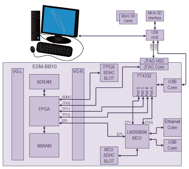
The ESM-BB10 board is attached to the Host Computer via a pair of USB cables. One USB cable attaches directly to the ESM-BB10 USB type B connector. This USB connection provides the CTY interface, TTY1 interface, TTY2 interface, and the Control Microcontroller programmer and debugger interface. On my system, this interface also powers the ESM-BB10 board.
The second USB cable attaches to the JTAG FPGA programmer which is plugged into the ESM-BB10 board. This interface is only required when making firmware updates to the KS10 FPGA.
These USB connections are illustrated below.
Download the binary distribution. The latest binary distribution is esm-bb10_binaries_160218.tar.gz (123 MB).
Untar the binary distribution into an empty directory as follows:
$ tar -zxvf esm-bb10_binaries_151228.tar.gz
Creating the Console Microcontroller SD Card
The SD Card that is used by the Console Microcontroller must be formatted with a FAT-32 filesystem. In order to save code size, I have configured the embedded filesystem to be read-only and to not implement long filenames – so it is best to avoid long filenames.
The files that have been created in the Host Computers diag directory must be copied to the diag directory of the SDHC Card. The unix cp command will work nicely provided your operating system supports the FAT-32 filesystem. The files in the diag directory must be copied to the diag directory of the SD Card in order for the Console Microcontroller software to find them.
mkdir /path/to/sdhc_card/diag
cp ./diag/*  /path/to/sdhc_card/diag
The installed filesystem looks like:
KS10> SD DIR
07/11/2013  08:43 PM           0 DIAG
04/21/2015  06:00 PM            25095 DIAG/DSKEA.SAV
04/21/2015  06:00 PM            18520 DIAG/DSKEB.SAV
04/21/2015  06:00 PM            15860 DIAG/DSKEC.SAV
04/21/2015  06:00 PM             8730 DIAG/DSKFA.SAV
04/21/2015  06:00 PM            32625 DIAG/DSDZA.SAV
04/21/2015  06:00 PM            11900 DIAG/DSKAA.SAV
04/21/2015  06:00 PM            13385 DIAG/DSKAB.SAV
04/21/2015  06:00 PM             9285 DIAG/DSKAC.SAV
04/21/2015  06:00 PM            10500 DIAG/DSKAD.SAV
04/21/2015  06:00 PM             7780 DIAG/DSKAE.SAV
04/21/2015  06:00 PM            10225 DIAG/DSKAF.SAV
04/21/2015  06:00 PM             4560 DIAG/DSKAG.SAV
04/21/2015  06:00 PM            20775 DIAG/DSKAH.SAV
04/21/2015  06:00 PM            23965 DIAG/DSKAI.SAV
04/21/2015  06:00 PM            16375 DIAG/DSKAJ.SAV
....
This SD Card should be inserted into the MCU SDHC Card Slot.
Creating the RP06 Disk Array SD Card
Unlike the SD Card that is used by the Console Microcontroller, the SD Card that is used by the RP06 Disk Array must be formatted with a PDP-10 filesystem. To accomplish this, we will binary copy a series of disk images to the RP06 SD Card.
At this point it is necessary to explain the SDHC Card partitioning which is very simple – each RP06 disk drive is allocated a 1 GB partition of the SDHC Card. The first RP06 disk, UNIT 0, occupies the first 1 GB. The second RP06 disk, UNIT 1, occupies the second 1 GB, etc. The fixed-sized 1 GB partitions makes the disk addressing simple and allows this partitioning scheme to work with the largest Massbus disk drives like the RP07. In this case, efficiency is complicated and storage is cheap.
The ESM-BB10 binary that you download should have three RP06 disk images: dskb.rp06, dskc.rp06, and red405a2.rp06. I think I got the TOPS-10 DSKB image and the DSKC image from https://www.steubentech.com/~talon/pdp10/. The TOPS-20 RED405A2 image is a RED Pack image that I created.
I should mention that creating your own RP06 disk images is simple. The RP06 disk format is exactly the same as SIMH. The following procedure loads DSKB: on UNIT 0, DSKC: on UNIT 1, and RED405A2 on UNIT 2.
Please read the following section very carefully.
Selecting the correct device for the SD Card is a little tricky under Cygwin. The procedure under Linux is similar. This is the procedure that I use.
Install the SD Card and type the following command:
$ cat /proc/partitions
major minor  #blocks  name   win-mounts

    8   160  31293440 sdk
    8   161  31289408 sdk1   G:\
    8     0 976762584 sda
    8     1 976759808 sda1   F:\
    8    16 976762584 sdb
    8    17    102400 sdb1
    8    18 976657408 sdb2   C:\
    8    32 2930266584 sdc
    8    33    131072 sdc1
    8    34 2930134016 sdc2   E:\
    8    48 2930266584 sdd
    8    49    131072 sdd1
    8    50 2930134016 sdd2   D:\
    8    64 976762584 sde
    8    65 976759808 sde1   K:\
    8    80   7744000 sdf
    8    81   7744000 sdf1
    8    96         0 sdg
    8   112         0 sdh
    8   128         0 sdi
    8   144         0 sdj
Because an 8 GB SD Card was inserted into the reader, it is plausible that /dev/sdf is the SD Card and is the correct device to write the disk image to.
So far, so good – but this needs to be verified. Next, unplug the SD Card from the reader and re-issue the same command:
$ cat /proc/partitions
major minor  #blocks  name   win-mounts

    8   160  31293440 sdk
    8   161  31289408 sdk1   G:\
    8     0 976762584 sda
    8     1 976759808 sda1   F:\
    8    16 976762584 sdb
    8    17    102400 sdb1
    8    18 976657408 sdb2   C:\
    8    32 2930266584 sdc
    8    33    131072 sdc1
    8    34 2930134016 sdc2   E:\
    8    48 2930266584 sdd
    8    49    131072 sdd1
    8    50 2930134016 sdd2   D:\
    8    64 976762584 sde
    8    65 976759808 sde1   K:\
    8    80         0 sdf
    8    81   7744000 sdf1
    8    96         0 sdg
    8   112         0 sdh
    8   128         0 sdi
    8   144         0 sdj
Note that size of /dev/sdf is now zero. That makes me even more confident that /dev/sdf is the correct device to write the image to.
Check, double check, and triple check that you have the correct device.
If you select the wrong device, this procedure will corrupt the destination disk drive and perhaps make your host computer unusable. You will certainly lose all of the data on that device.
If you are not completely comfortable with this warning, STOP NOW!
Reinstall the SD Card into the reader.
The following procedure must be performed with Administrator Privileges under Cygwin and must be performed with Root Privileges under Linux. You’ve been warned twice.
Using the device name identified above (instead of what is shown in the webpage below), write the RP06 disk images to the SD card using the dd command as follows:
$ dd if=dskb.rp06 of=/dev/sdf bs=512 iflag=count_bytes oflag=seek_bytes count=309700K seek=0G
615600+0 records in
615600+0 records out
315187200 bytes (315 MB) copied, 393.541 s, 801 kB/s
$ dd if=dskc.rp06 of=/dev/sdf bs=512 iflag=count_bytes oflag=seek_bytes count=309700K seek=1G
615600+0 records in
615600+0 records out
315187200 bytes (315 MB) copied, 408.371 s, 772 kB/s
$ dd if=red405a2.rp06 of=/dev/sdf bs=512 iflag=count_bytes oflag=seek_bytes count=309700K seek=2G
427624+0 records in
427624+0 records out
218943488 bytes (219 MB) copied, 273.721 s, 800 kB/s
Install this SD Card into the FPGA SDHC Slot.
Programming the KS10 Console Software
The KS10 Console software is stored in Flash Memory internal to the Texas Instruments/Stellaris LM3S9B96 Microcontroller. The ESM-BB10 board has an FTDI FT4232H (Hi-Speed Quad USB UART) chip on-board and is designed such that Port A of the FT4232 is connected to the JTAG port for the Console Microcontroller. The Microcontroller chip is programmed via this JTAG interface using the OpenOCD application. An in-circuit emulator/debugger can also use OpenOCD and this JTAG interface to debug the console software.
The following line in the makefile will probably need to be modified to match the path of your OpenOCD installation.
OPENOCD := \
	/usr/local/openocd-0.8.0/bin/openocd-0.8.0.exe
Once the makefile is modified, the Console Microcontroller software is programmed simply by executing the make load_code command.
$ make load_code
/usr/local/openocd-0.8.0/bin/openocd-0.8.0.exe -f ks10.cfg -c "program_device ()"
Open On-Chip Debugger 0.8.0 (2014-04-28-08:39)
Licensed under GNU GPL v2
For bug reports, read
        https://openocd.sourceforge.net/doc/doxygen/bugs.html
Info : only one transport option; autoselect 'jtag'
adapter speed: 500 kHz
Warn : Using DEPRECATED interface driver 'ft2232'
Info : Consider using the 'ftdi' interface driver, with configuration files in interface/ftdi/...
Info : max TCK change to: 30000 kHz
Info : clock speed 500 kHz
Info : JTAG tap: lm3s9b9x.cpu tap/device found: 0x4ba00477 (mfg: 0x23b, part: 0xba00, ver: 0x4)
Info : lm3s9b9x.cpu: hardware has 6 breakpoints, 4 watchpoints
Info : JTAG tap: lm3s9b9x.cpu tap/device found: 0x4ba00477 (mfg: 0x23b, part: 0xba00, ver: 0x4)
target state: halted
target halted due to debug-request, current mode: Thread
xPSR: 0x61000000 pc: 0x02000c22 psp: 0x200014e0
DEPRECATED! use 'cortex_m' not 'cortex_m3'
cortex_m interrupt mask on
auto erase enabled
wrote 59392 bytes from file ./console.bin in 9.311533s (6.229 KiB/s)
verified 58608 bytes in 0.920052s (62.208 KiB/s)
DEPRECATED! use 'cortex_m' not 'cortex_m3'
cortex_m interrupt mask off
requesting target halt and executing a soft reset
Warn : soft_reset_halt is deprecated, please use 'reset halt' instead.
target state: halted
target halted due to breakpoint, current mode: Thread
xPSR: 0x01000000 pc: 0x01000c4c msp: 0x20000800
shutdown command invoked
Programming the KS10 FPGA Firmware
The KS10 FPGA firmware is stored in a serial Flash Memory device on the ESM-BB10 KS10 board and is programmed via the JTAG link. Programming the serial Flash Memory device using the GUI is an interesting process which is not recommended for the timid. I’ve automated the programming process in the makefile.
The following line in the makefile will probably need to be modified to match the path of your Xilinx installation.
IMPACT := \
	/cygdrive/c/Xilinx/14.7/ISE_DS/ISE/bin/nt64/impact.exe
Once the makefile is modified, the serial Flash Memory is programmed simply by executing the make load_fpga command.
$ make load_fpga
/cygdrive/c/Xilinx/14.7/ISE_DS/ISE/bin/nt64/impact.exe -batch esm_ks10_impact.cmd
Release 14.7 - iMPACT P.20131013 (nt64)
Copyright (c) 1995-2013 Xilinx, Inc.  All rights reserved.
Preference Table
Name                 Setting
StartupClock         Auto_Correction
AutoSignature        False
KeepSVF              False
ConcurrentMode       False
UseHighz             False
ConfigOnFailure      Stop
UserLevel            Novice
MessageLevel         Detailed
svfUseTime           false
SpiByteSwap          Auto_Correction
AutoInfer            false
SvfPlayDisplayComments false
INFO:iMPACT - Digilent Plugin: Plugin Version: 2.4.4
INFO:iMPACT - Digilent Plugin: Opening device : "JtagHs2".
INFO:iMPACT - Digilent Plugin: User Name: JtagHs2
INFO:iMPACT - Digilent Plugin: Product Name: Digilent JTAG-HS2
INFO:iMPACT - Digilent Plugin: Serial Number: 210249854216
INFO:iMPACT - Digilent Plugin: Product ID: 30900152
INFO:iMPACT - Digilent Plugin: Firmware Version: 0108
INFO:iMPACT - Digilent Plugin: JTAG Port Number: 0
INFO:iMPACT - Digilent Plugin: JTAG Clock Frequency: 10000000 Hz
Identifying chain contents...'0': : Manufacturer's ID = Xilinx xc6slx45, Version : 2
INFO:iMPACT:1777 -
   Reading C:/Xilinx/14.7/ISE_DS/ISE/spartan6/data/xc6slx45.bsd...
INFO:iMPACT:501 - '1': Added Device xc6slx45 successfully.
----------------------------------------------------------------------
----------------------------------------------------------------------
done.
Elapsed time =      0 sec.
Elapsed time =      0 sec.
Elapsed time =      0 sec.
Elapsed time =      0 sec.
Unprotect sectors: FALSE
INFO:iMPACT - A CFI file is not detected. To ensure correct and safe
   configuration,
    Please make sure a CFI file is present in the same directory as the PROM
   file,
    or, regenerate the PROM file with the latest software.
Maximum TCK operating frequency for this device chain: 25000000.
Validating chain...
Boundary-scan chain validated successfully.
'1': SPI access core not detected. SPI access core will be downloaded to the
device to enable operations.
INFO:iMPACT - Downloading core file
   C:/Xilinx/14.7/ISE_DS/ISE/spartan6/data/xc6slx45_spi.cor.
'1': Downloading core...
 LCK_cycle = NoWait.
LCK cycle: NoWait
done.
'1': Reading status register contents...
INFO:iMPACT:2219 - Status register values:
INFO:iMPACT - 0011 1100 1110 1100
INFO:iMPACT:2492 - '1': Completed downloading core to device.
'1': IDCODE is '15' (in hex).
'1': ID Check passed.
'1': IDCODE is '15' (in hex).
'1': ID Check passed.
'1': Erasing Device.
'1': Using Sector Erase.
'1': Erasing non-volatile quad-enable bit...
'1': Programming Flash.
'1': Reading device contents...
done.
'1': Verification completed.
INFO:iMPACT - File esm_ks10.cfi does not exist.
'1':Programming in x1 mode.
S25FL032P Status Register Contents = 0x0000.
QUAD ENABLE                                       :         0
STATUS REGISTER PROTECT 1                         :         0
STATUS REGISTER PROTECT 0                         :         0
SECTOR PROTECT                                    :         0
TOP/BOTTOM PROTECT                                :         0
BLOCK PROTECT BIT 2                               :         0
BLOCK PROTECT BIT 1                               :         0
BLOCK PROTECT BIT 0                               :         0
'1': Programmed successfully.
INFO:iMPACT - '1': Flash was programmed successfully.
 LCK_cycle = NoWait.
LCK cycle: NoWait
INFO:iMPACT - '1': Checking done pin....done.
'1': Programmed successfully.
Elapsed time =     63 sec.
When the Firmware has been programmed successfully, you will need to reset the Console Microcontroller. The Console Microcontroller will reprogram the FPGA with the new firmware at startup. The Console Microcontroller can be reset via the JTAG link by executing the make reset command as follows:
$ make reset
/usr/local/openocd-0.8.0/bin/openocd-0.8.0.exe -f ks10.cfg -c "reset" -c "shutdown"
Open On-Chip Debugger 0.8.0 (2014-04-28-08:39)
Licensed under GNU GPL v2
For bug reports, read
        https://openocd.sourceforge.net/doc/doxygen/bugs.html
Info : only one transport option; autoselect 'jtag'
adapter speed: 500 kHz
Warn : Using DEPRECATED interface driver 'ft2232'
Info : Consider using the 'ftdi' interface driver, with configuration files in interface/ftdi/...
Info : max TCK change to: 30000 kHz
Info : clock speed 500 kHz
Info : JTAG tap: lm3s9b9x.cpu tap/device found: 0x4ba00477 (mfg: 0x23b, part: 0xba00, ver: 0x4)
Info : lm3s9b9x.cpu: hardware has 6 breakpoints, 4 watchpoints
Info : JTAG tap: lm3s9b9x.cpu tap/device found: 0x4ba00477 (mfg: 0x23b, part: 0xba00, ver: 0x4)
adapter speed: 500 kHz
cortex_m reset_config vectreset
Resetting Core Peripherals
Info : JTAG tap: lm3s9b9x.cpu tap/device found: 0x4ba00477 (mfg: 0x23b, part: 0xba00, ver: 0x4)
Warn : Only resetting the Cortex-M core, use a reset-init event handler to reset any peripherals or configure hardware srst support.
Software and Firmware Development
Software and firmware development requires a laundry list of tools.
An incomplete list of tools that I use is summarized below. You are welcome to substitute your favorites – but these work for me!
- Linux (or Cygwin) GNU development system including:
- GCC compiler collection for ARM processors. The compiler I use is:
$ arm-none-eabi-gcc –version
arm-none-eabi-gcc (GCC) 4.7.2
Copyright (C) 2012 Free Software Foundation, Inc. - make
- rcs
- awk
- GCC compiler collection for ARM processors. The compiler I use is:
- Xilinx ISE 14.7 Webpack
- iverilog-20130827
- Digilent JTAG HS2 Programming Cable
- Digilent Plugin for Xilinx Tools
- Open On-Chip Debugger (openocd-0.8.0)
- FTDI USB drivers.. This driver is required for the serial interface and for openocd.
I use cygwin-based tools for development. I also use rcs for configuration management. The RCS information in the source tree can be ignored unless you are interested in ancient history.
I use iverilog for the regression test suite. It compiles the Verilog HDL code much faster that the Xilinx Fuse tool and executes about twice as fast. If I want to see the simulation waveforms, the Xilinx simulator is better.
Building the KS10 FPGA software and firmware:
I’ve temporarily removed the build instructions from the website, but I’ve included pre-built binaries that can be used.
I doubt anybody but me could build the system anyway.
What needs to be done?
If you’d like to contribute to the software design of the firmware design, please contact me. There is plenty to do! The following is a small summary of the Things To Do list:
- Software projects (all low priority):
- lwIP is working. It would be nice to have the DZ11 terminals and the CTY available via Telnet/Ethernet.
- KS10 networking?
- FPGA (verilog) projects:
- There are a lot of synthesis warning during the build process. This needs to be cleaned up.
- There are a couple of combinational loops (false paths) that are part of the KS10 design. Although the microcode does not enable these paths, they confuse the timing analysis. Rather than figure this all out, I’ve removed these paths from the timing analysis with sledgehammer-like precision. This needs to be cleaned up.
Downloading the Design:
Version 00.07 of the KS10 FPGA design can be downloaded from: ks10_all_dist_150521.tgz (appx 111 Mb). This is the first version of the FPGA firmware that will actually execute code.
The design is documented in the KS10 FPGA Processor Manual (Rev 40) (2.4 Mb).
Previous Revisions:
Version 00.06 of the KS10 FPGA design can be downloaded from: ks10_all_dist_150403.tgz (appx 34 Mb).
Version 00.05 of the KS10 FPGA design can be downloaded from: ks10_all_dist_140105.tgz (appx 11 Mb).
Version 00.04 of the KS10 FPGA design can be downloaded from: ks10_all_130529.tgz (appx 0.5 Mb).
Version 00.03 of the KS10 FPGA design can be downloaded from: ks10_all_130105.tgz (appx 4.4 Mb).
Version 00.02 of the KS10 FPGA design can be downloaded from: ks10_all_121210.tgz (Happy DEC 10 Day!) (appx 1.3 Mb).
Version 00.01 of the KS10 FPGA design can be downloaded from: ks10_all_121120.tgz (appx 2.8 Mb).
Acknowledgements:
I would like to thank Keith for generously providing web hosting for this project and Emanuel for providing the prototype hardware! It is greatly appreciated.
I would also like to thank Rich Alderson and the folks at the Living Computer Museum for digging up the various diagnostics programs and Timothe Litt (one of the KS10 engineers at DEC) for answering countless questions about KS10 systems and software.
Contacts:
If you have any comments, questions, suggestions, or don’t understand something, please contact me.
Rob Doyle
doyle (at) cox (dot) net
Hi Rob. I find what you are doing interesting. If you maintain an interested parties list please put me on it.
I used a TOPS-10 system on a KL10 back in the early 80’s at the University of Queensland Australia.
I have much to learn if I were to attempt to reproduce what you are attempting. My experience was only as a student user.
Reading about how you are attempting to construct a CPU that will maintain compatibility with the original microcode prompts me to ask.
What level of microcode are you using? Where did you get it? Where could I get it?
Why did you choose a KS instead of the KL? Was it just because it would be smaller and simpler. Was it to avoid memory management issues?
I have started to read your project manual and noted you said the microcode ROM was 4K by 108 bits. I found this document on bitsavers https://bitsavers.trailing-edge.com/pdf/dec/pdp10/KS10/TOPS-10onThe2020_Mar79.pdf where on page 16 it says 96 bits. Can you say why the difference?
Also why was the ALU implemented as 10 4bit slices and not 9 as I would have assumed for a 36bit CPU?
Would you consider adding a suggested reading list to your project? I think that would help people like me in attempting to “get my head around” what you are doing. If it is not too long that is.
I shall check back on progress. Good luck with it.
Q: What level of microcode are you using? Where did you get it? Where could I get it?
A: I’m using the last revision of the microcode – version 130. I have an AWK script that parses the microcode listing file and creates the Control ROM (Microcode) and the Dispatch ROM. The microcode listing is available from:
https://pdp-10.trailing-edge.com/ksu2_130/01/ks10.mcr.html
There is a hack to this microcode to support MIT ITS that is available at:
https://www.dbit.com/pub/pdp10/ks10/mcr.262
Q: Why did you choose a KS instead of the KL?
A: The KS10 is just simpler. It is supported by SIMH which is useful as a reference.
Q: I have started to read your project manual and noted you said the microcode ROM was 4K by 108 bits. I found this document on bitsavers https://bitsavers.trailing-edge.com/pdf/dec/pdp10/KS10/TOPS-10onThe2020_Mar79.pdf where on page 16 it says 96 bits. Can you say why the difference?
A: Perhaps sloppy terminology on my part. If you look at the microcode listing file referenced above, the Control ROM output (microcode) is 108-bits wide.
In a real DEC KS10, the microcode output is post-processed. The microcode bits are rearranged – I suppose to simplify the circuit board layouts. Also some microcode fields bits are just removed. I think that they are present for some kind of a simulator and/or special debug hardware that is not present on production systems. I think it also adds parity to the microcode word.
Therefore the memory width in the actual hardware is different than the memory width in the microcode documentation…
This is documented in Figure 5-20 in the KS10 Technical Manual – if you know what you’re looking for. See below for download information on that manual.
The KS10 FPGA design doesn’t do any of that. It just defines the 2K x 108 bit ROM. No need to rearrange anything. Also the HDL synthesis tool is smart enough to discover that some microcode fields are unused and the tool just removes them. It is just simpler that way.
Q: Also why was the ALU implemented as 10 4-bit slices and not 9 as I would have assumed for a 36-bit CPU?
A: Strange isn’t it? I pondered that for a long time.
The ALU is sign extended by two bits on the left, and zero padded by two bits on the right.
The ALU is implemented with am2901 4-bit slice processors. This implementation gives the hardware access to the CRY2 (Carry 2) signal which is available at the interface between the first and second ALU chip. If this was implemented as a 36-bit wide ALU, this signal would be buried deep inside the one of am2901 chips and not accessible.
The CRY2 signal is necessary to create one of the PDP10 arithmetic flags.
Q: Would you consider adding a suggested reading list to your project? I think that would help people like me in attempting to “get my head around” what you are doing. If it is not too long that is.
A: Download the “DEC Documents” link is the “Downloading the Design” section on this webpage.
Hi, Haven’t seen an update in a while. Was just wondering what the status of the project is?
Any updates?
I don’t really maintain this site anymore.
See https://github.com/KS10FPGA/KS10FPGA
Hello,
I try implement the ks10 and get error on that ubaloop.v is missing, I used the latest archive.