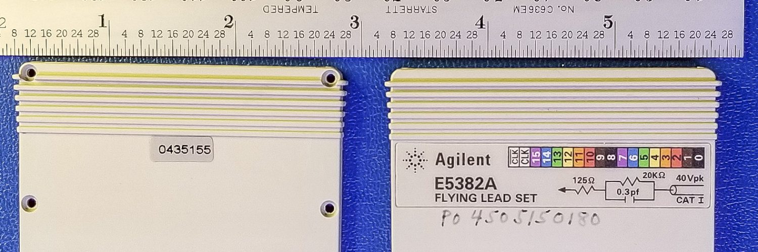
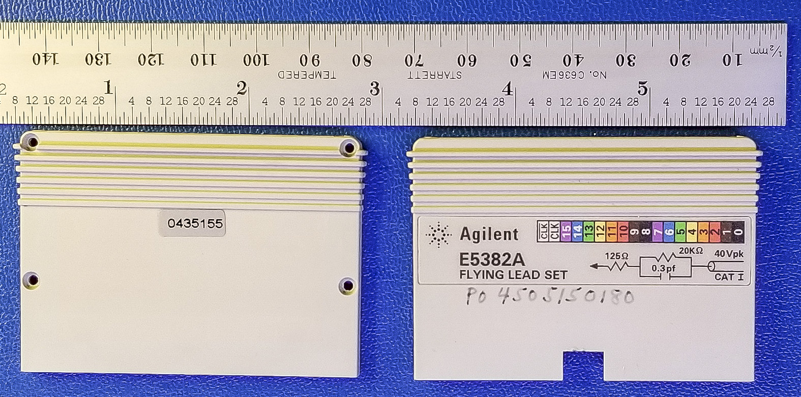
I recently tore down an Agilent E5382A Flying Lead Set. I used a Torx T-4 bit to remove the (4) tiny tiny screws.
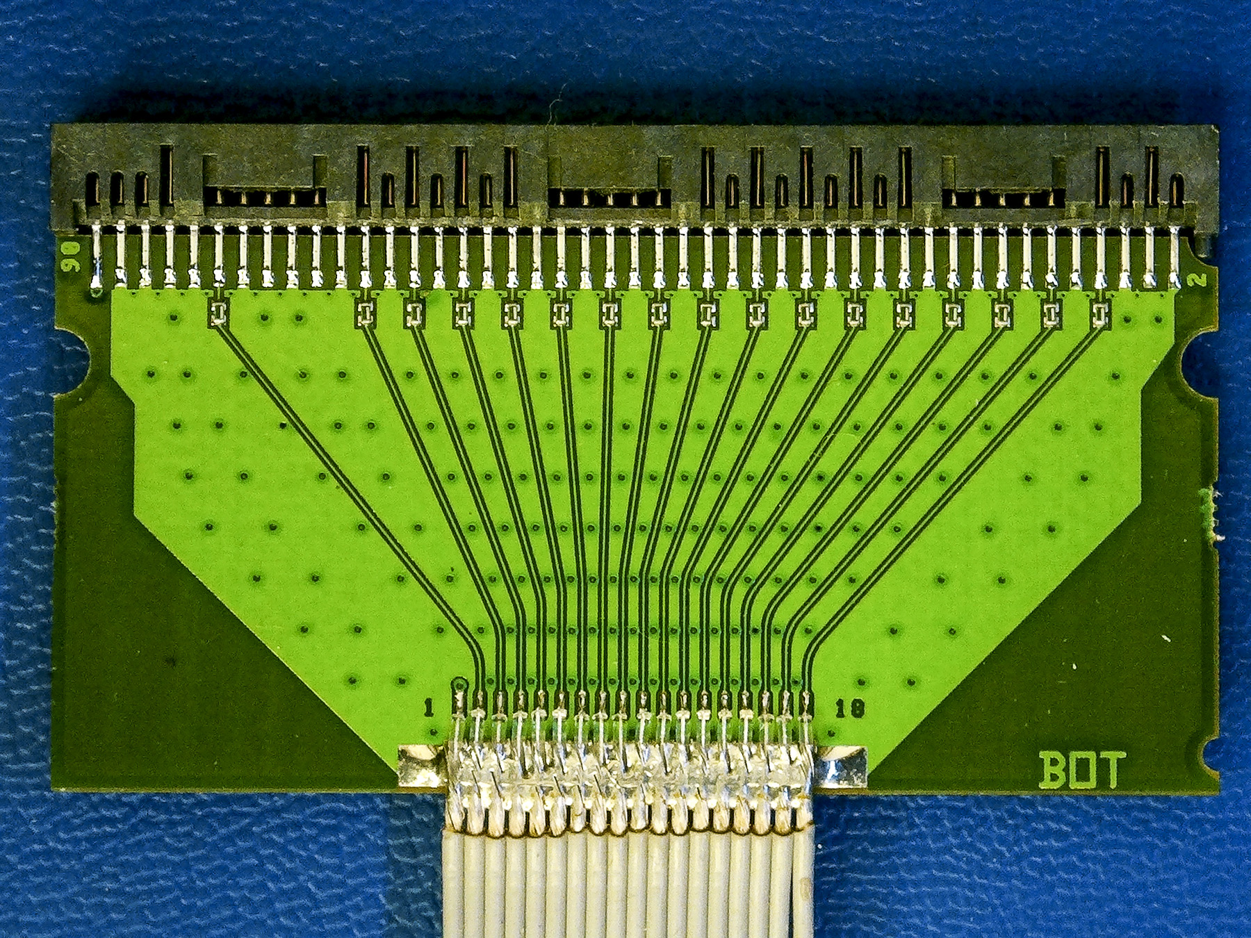
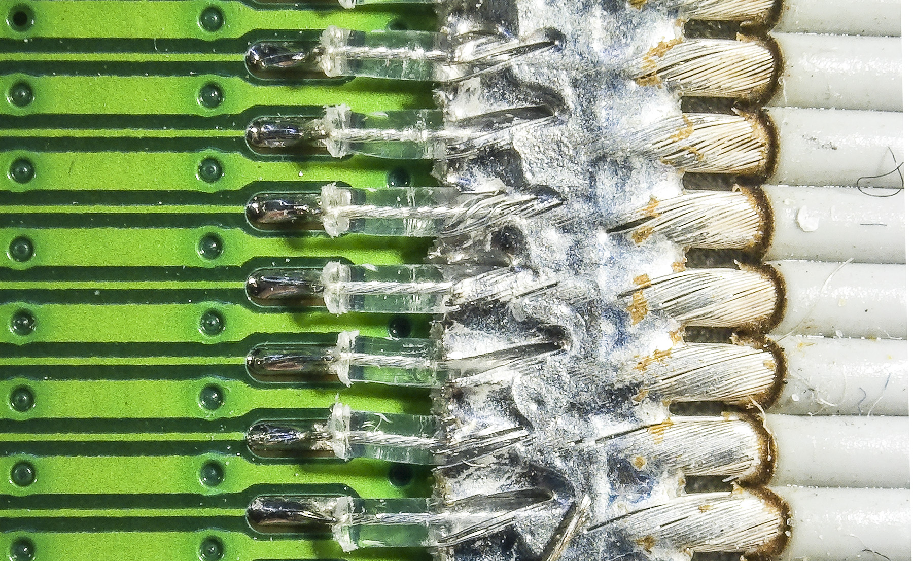
This adapter has a 90-pin connector that comes from HP logic analyzer cards, and then goes out to single ended flying leads for direct connection to the System Under Test.
[…] my post here you can also see another example of similar construction from Agilent on one of their pods. That […]
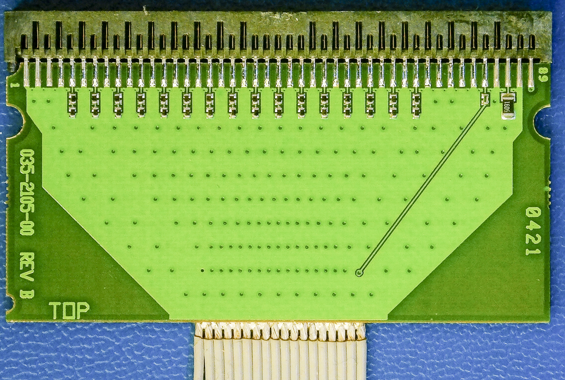
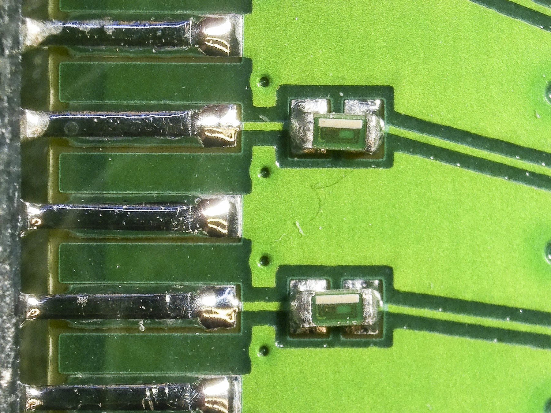
You’ve very nicely provided the resistance of all of the resistors, but not any information on the component that is in series with the signal lines. Can you provide some info on that? It doesn’t look like a resistor. In fact, it almost looks like a microscopically small circuit board, so I’m wondering if it is a custom component?
Hi Alan,
I don’t really know what they are! My omission wasn’t accidental! 🙂
Perhaps something like this ESD protection device?Let me ask a couple friends who might have a better idea. My knowledge of analog components, design, etc is particularly weak.
(see my response below which should help)
Thanks
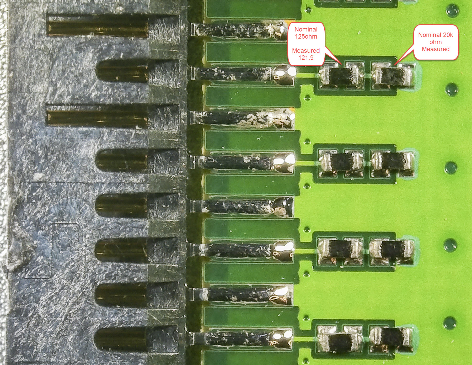
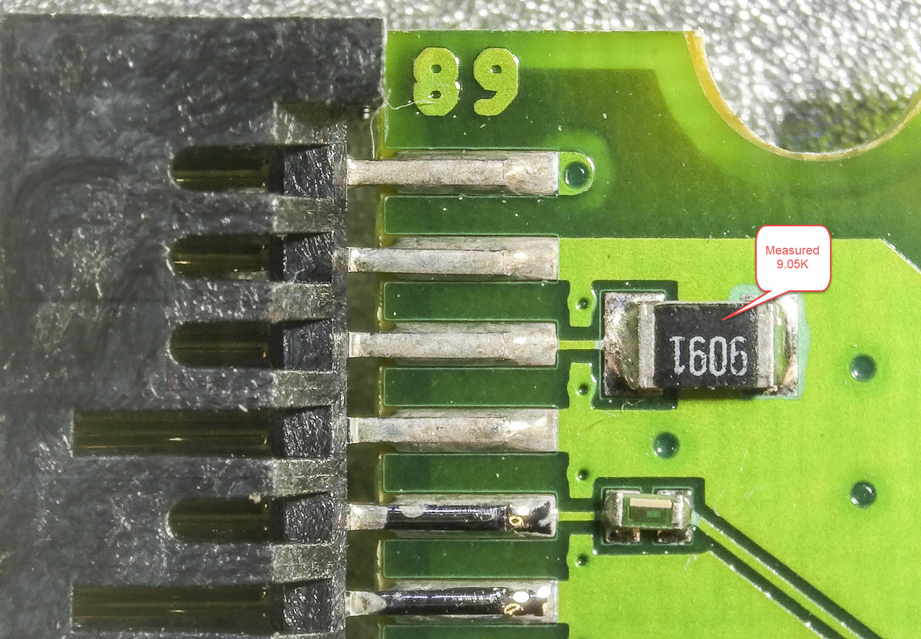
OK…. That is kind of a stupid question. 🙂 The case shows a 0.3pF cap, so I assume that is what we’re looking at. However, that doesn’t completely solve the mystery for me. The schematic shown on the case doesn’t appear to correlate with the actual wiring, so I’m guessing that the schematic is an ‘effective system’ reflective of what you can expect, and not explicit components. The double resistors to ground are not even on opposing sides of the board (I’m thinking… maybe I’m missing a via…). It really looks as though the signals come in from the flying lead connector (1 – 18), through a single series component, and then into the 90 pin connector of the probe head.
My original assumption was also that it was a capacitor — and labeled my photos as such. I figured it had to be given the diagram you mentioned. However, I’ve never seen a capacitor like that in my travels, and held back from specifically saying that as a result.
My second guess was that it was an inductor, just given the nature of that spiral trace that’s visible. Looks like a coil, maybe it is one. When I read more about inductors, though, I had a problem matching the common applications to this one. But nothing should be too surprising to the unlearned!
My smart friends tell me that it IS an inductor, possibly made by Wurth Elektronik or Abracon, with the purpose of slowing down the edge of signal transitions in this application. A guess puts it at 3nH, but the exact value may not be critical.
The schematic on the adapter (photo 1) shows a 0.3 pF cap in parallel of the 20K resistor and not a coil. This is to help fast transients to be reproduced more accurately by shortly bypassing the RC constant (R=20 kOhms and C being the logic analyzer input capacitance)
Actually, now that I look closely at the mechanicals of the pins, the pins are staggered from the components on the top layer to the components on the bottom layer, so they are likely not connected, unless the vias were blind, but I doubt that. Just the two Rs seem strange.
Thank you very much for doing this. Those components on the top that are guessed to be Ls do make sense, because a C would not work, that would block DC, and you want DC to pass. Unless there was a connection between the top and bottom components. Do you still have that pod and could check that? Thank you very much. Austin
Hey good morning Austin. I do still have that pod. I haven’t really touched this for a few years, though. Can you be a bit more specific about what you want me to tone out? Like whether the two resistors connect to that possible-inductor on the other side?
I guess I’d be surprised. But I can look. Feel free to nudge me if I forget…. I’ve got a new PCB that I ordered coming in this week, components, etc and I’m reversing another PAL at the moment as well…. busy!
Hi Keith, Whether either end of the 125Ohm resistor has connection to either side of the inductor on the signal side. I don’t think it will, just because the pins/components are staggered from their mated signal/return channels, but it’s worth a try. Thanks! Austin
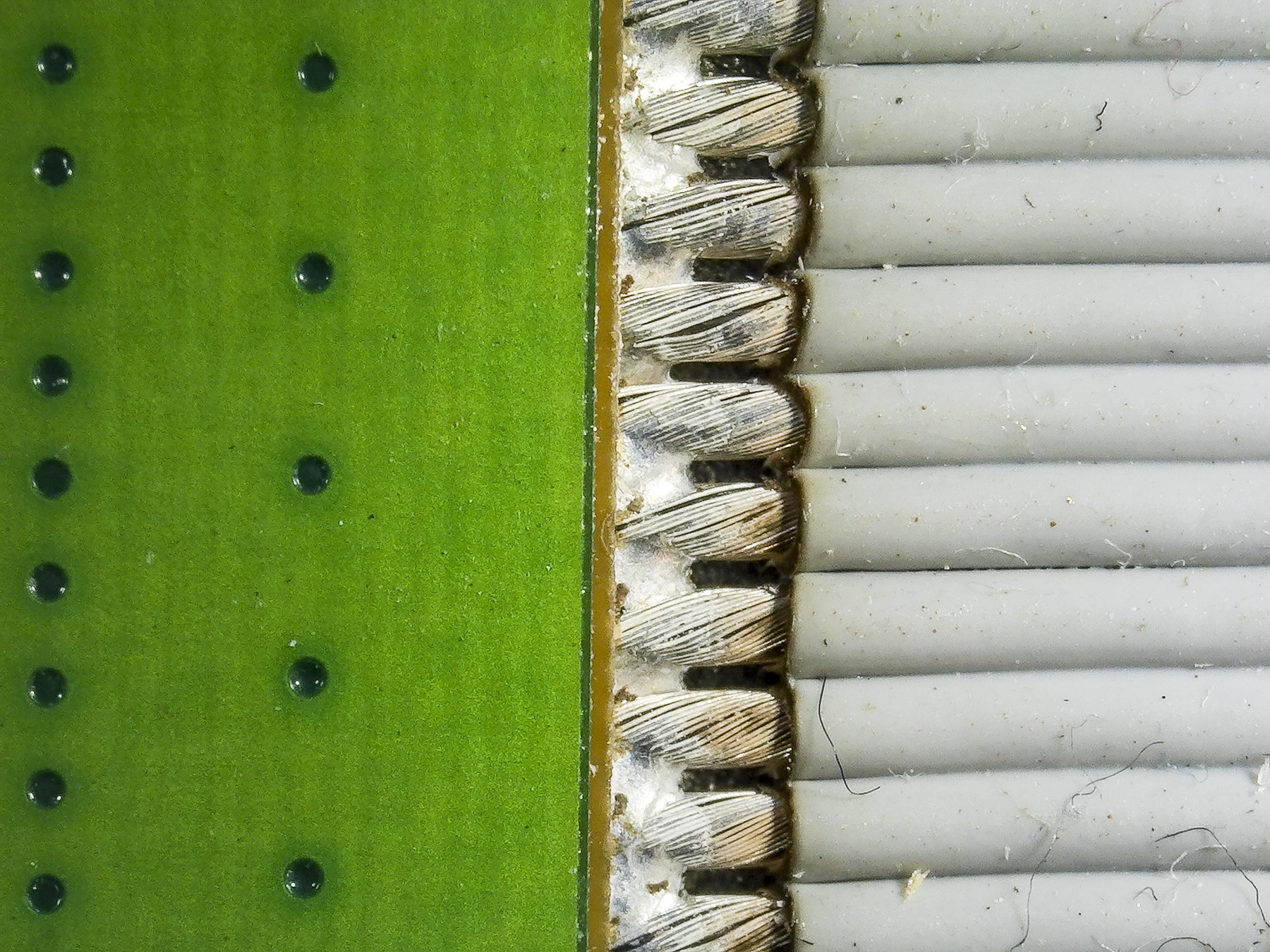
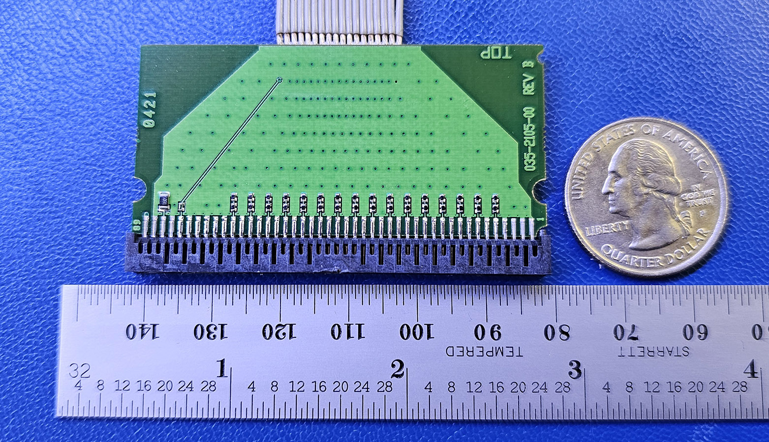
This is just about the smallest thing I’ve ever probed. Surprised I got good measurements before. I added a new photo to the gallery with a quarter for scale. The older images really don’t give you an idea.
The answer is no — neither side of the 125ohm resistor connect to either side of the inductor.
Again, thank you very much! My guess was those Rs and the Ls were 0402s, and the larger one was an 0805. Do you think those are 0402s?
Yeah doing the pixel math I’m coming up with 0805’s (1.23mm width) for the large resistor, and 0402’s(0.47mm width) for the smaller ones.
Thank you! Those pods are very expensive, and as I need 8 of them, I am thinking of spinning a board to make my own probes that will mount in a less expensive probes housing, and use some other 4G probe wires that I have for another analyzer card (these probe wires are nearly identical to the ones on the E5382A pods). Those analyzer cards are 4G, just limited # of signals (8 per card at 4G) and doesn’t have the eye scan feature of the 1657xA cards. I think I can make each 16 channel probe for around $250 or less, as opposed to $800+. More reasonably priced E5382A pods do show up every now and then, but few and far between.
I think the mystery components are polyfuses.