So, as I mentioned in another post, I added Jim Thompson’s phase-jerked-loop to the project. Phil had good luck using it with his DiscFerret, but it really didn’t help me. My problem disks are still problem disks. And the data returned as a result still have the same problem.
This PJL really didn’t help me.
https://www.analog-innovations.com/SED/FloppyDataExtractor.pdf
I expected the numbers to look a little more stable —- as if we are tracking them better, but I really just didn’t see this.
I’m planning on reverting my changes soon unless some more playing around will help.
Hello!
Well done! Its a great project, I’ve been following for long time. I’m trying to make some emulation stuff recently with my ARM. But unfortunatelly encountered problem with STEP signal. My uP doesn’t see it. I have no logic analyzer, its a shame of course. I’m able to catch DS and DIR signal, but not STEP. Have you encoutered similar problems in your project ?
Regards,
Greg.
Hi Greg,
So are you trying to “sniff” or watch an existing controller or something?
Step signals can be very very small in pulse width. The pulse width can be as small as .8 microseconds with about a 3ms interval between them. What frequency does your uP run at? Are you using some form of edge detection, or sampling?
Can you be more specific about how you are “catching” these signals?
Hello again,
ok 🙂 I made iterrupt handler to catching rising and falling edges for (DS and STEP signals). Inside this handler I count the occurence of those signals changes. DS is countig quite fine, but STEP is not, at all. I tried to connect DS input (ARM side) to some pins in 34 floppy connector. Its counting for DS and DIR but not for STEP regardless of whether I connect it to pin 20 directly (without floppy) or sniff working floppy.
ARM run at 55MHz thats why I didnt expect any problems with catching these signals. 0.8usec should be enough to be seen by uP. Maybe I need to re-study ARM hardware specification…. In theory STEP signal must be there 🙂 but I can’t prove it as long as I have available so limited resources.
Just remember that if you attach directly to the floppy, that for signals coming FROM the floppy (not the case with STEP), that you need a 1k pullup resistor or you won’t see crap.
If you are just watching the STEP signals between the controller and the drive, if the drive is stepping (listen and feel), then the pulse is getting there. 🙂
I’d double check all your interrupt logic especially when it comes to what happens when multiple interrupts happen. Do they get queued? Or dropped? and so on.
If you take the step pin and just touch it to +5v and release, you should hear the drive step.
OK 🙂 eventually I could manage with it. STEP signal exists in fact 🙂
From now on it should be much much easier 😉 just read SD, encode to mfm and send data to floppy 🙂
Thanks for your help!
Hi
I am planning to make the emulator of floppy on STM32 ARM.
There is another project that emulates both read and write on PIC uP and SD card. But it isnt open.
I implemented the digital PLL to FPGA finally. It is the same circuit I described few articles back. It seems to be stable. Here is the result:
RD is read signal from floppy
rdc is clock output from separator
rdd is data output from separator
I am using the invertors with schmitt triggered inputs – 74C14 between FPGA and floppy. That’s why RD polarity is incorrect. Together with pullup resistors on inputs from floppy it improves the data slightly. 5 1/4″ drives does not work without them, because they always have open collector outputs.
How to shift them to the shift register now? Does the rdd pulses that came during rdc=’0′ belong to clock and the ones that came during rdc=’1′ to data (or vice versa)?
Hi again omikron.
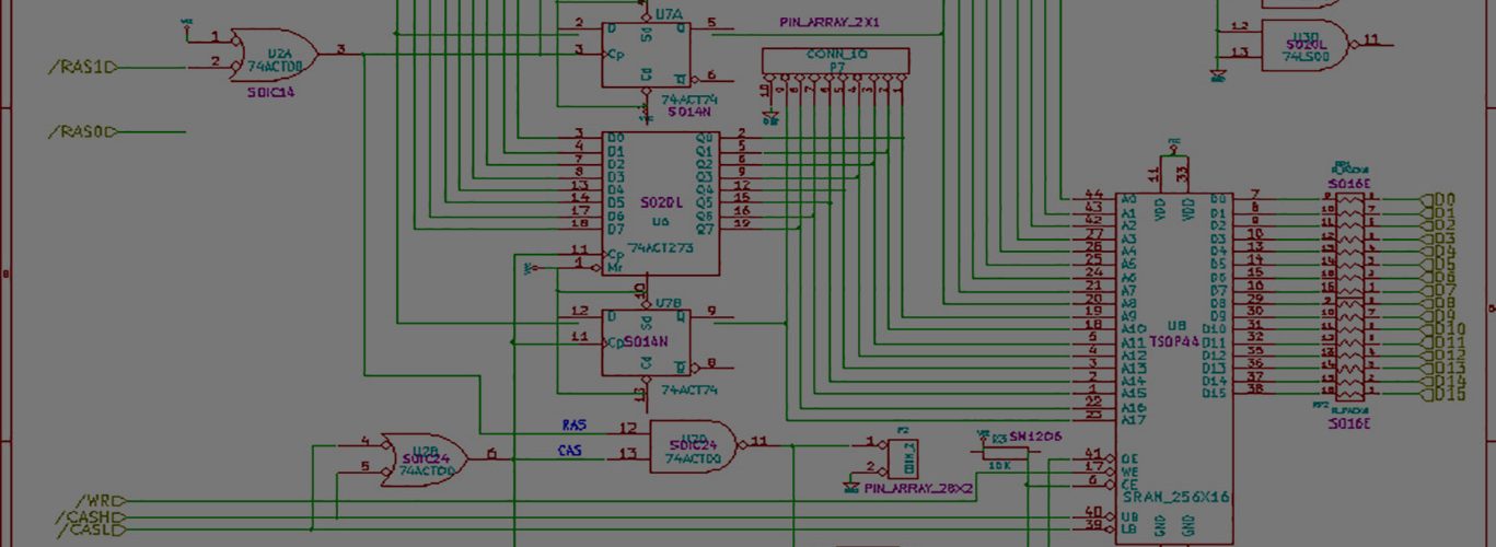
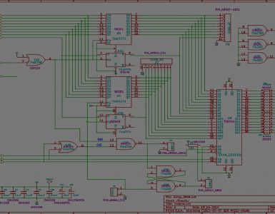
When you said you implemented the digital PLL to FPGA, how did you do it? Just via a schematic capture? or verilog, or vhdl? For Xilinx?
For your picture, I really don’t know what I’m looking at. I don’t necessarily see a relationship between the rdc and the rdd. If you are outputting a read clock (or even a read window), then I’d expect there to be one.
If you are dealing with 2us bit cells, then you need to save one bit of raw MFM for each bit cell. In order to tell the difference between a clock bit and a data bit, you need to first find the sync, and then the first bit after the sync is a clock bit. Unless you are doing sync’ing in hardware, you basically need to capture all the bits and then post-process them.
Note there are multiple ways to achieve the same result. For instance, you can start a timer on a negative-going edge, and stop it on the next edge, and transfer “delta t’s.” You can then convert the time between edges into raw MFM.
Hope this helps. If it doesn’t, reply back, and we’ll try again! 🙂
It is in VHDL on Digilent’s Nexys2 board. It uses the 1200 cells Spartan3E. I am writting the shift register and comparator right now. I’ll send you the sources then.
YES, I just tested the shift register+pattern comparator and I can detect 11 matches with 0x4489 on EVERY floppy turn.
Now is the time to write something like FIFO, which will collect the 16bit raw symbols and send them to PC
Oh the nexys2 board, yeah, I know that one! You have the 1200K one, huh? I’ve also got the spartan 3e, but the 500k gate one. Which is fine for me right now. I haven’t come even close to capacity with my projects.
I have my verilog code in the download section of my blog, if you are interested.
I’m glad to see you are detecting the syncs — very important first step. I’m guessing then you are doing amiga disks? Most of the commenters here are usually doing PC or something else.
Fantastic in any case. I use a FIFO(using block rams) and send the data to the PC in real time. It’s much faster than read-store-transfer method.
Hi
Here is my implemetation:
https://www.tomas-franke.cz/speccy/floppy.zip
I am not sure that the fifo is written correctly.
And here is the sample of raw zero track of Amiga Floppy made by this circuit:
https://www.tomas-franke.cz/speccy/sample.zip
It has some remapping, see shreg.vhd file
But I don’t know how to extract the sectors from these raw data, do you?
I’m taking a look at your sample and there’s definitely something not right there. I first thought that you just weren’t properly bit-aligned with the syncword. Before you can perform the decoding, each sector must be properly aligned. You’ll generally have two alignments — the first whole sector will have one alignment, and the first sector after the gap will have a different alignment.
I also tried block shifting left and right a bunch of times and searching for “0x94489” where I should find exactly 11 sectors. Your file size seems weird too. It’s 32k, right? If you are capturing one whole track, you should have around 11k +/- depending on how much over the 200ms you captured.
I don’t think you have raw MFM there. What mainly makes me think this is that your character distribution is all over the place. There are only 32 possible raw MFM data bytes:
https://techtravels.org/?p=62
I still have to look at your VHDL — although I don’t know it and might struggle a little bit, maybe something will jump out at me.
I made bit remapping in shreg.vhd. There are clocks between data bits: CDCDCDCDCDCDCDCD. In this file they are DDDDDDDD CCCCCCCC to make the software process easier.
Hrrrrmm. I think you’re going to find it easier if you leave the clock bits and data bits intact and then mask them away during the decoding process.
I’ve always worked with them combined in the RAW MFM stage, so your file looks pretty foreign to me. Sorry.
I made some changes tonight. I found the timing hazard and comment out the bit remmaping also. It looks much more like the article about MFM coding now. The data are stored in array [] of word format now, the Low byte comes first and then Hi.
So, look for 89 44 instead of 44 89.
I re-uploaded the files to my server.
How can I decode the sector data from the raw words?