I’ve just managed to get some key components working this year, and as a result, the machine is becoming more usable.
I wanted to measure the performance of this Frankenstein machine. Ideally, I’d use standardized benchmarks but I don’t really have a compilation toolchain setup yet. I’m mostly stuck using 68K assembly.
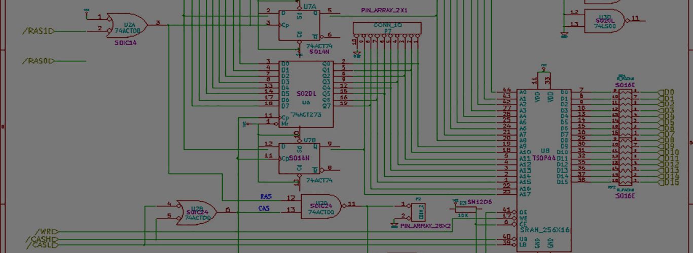
I am in the process of investigating vbcc to use with vasm, the assembler I’m using now to create machine code for this beast. Remember that while someone else created the J68 soft-cpu, that I’ve written the memory controllers and/or glue logic. This includes the interface with the video frame buffer.
I’m using four types of memory currently:
- 4MB SRAM for the frame buffer. During CPU access, the video driver is blocked from reading it — or more accurately, just temporarily displays the CPU data randomly on the screen. I think this side-effect looks neat.
- 8MB SDRAM using a ported memory controller. This is generic RAM.
- Some portion of FLASH memory, the so-called User Flash Memory, which currently holds the code. Which is specifically VUBUG.txt.
- Some portion of FPGA block memory, the m9k’s, which holds microcode, registers, and so on. Also an amount for working RAM.
The design decisions surrounding memory architecture, video frame buffer, and general bus connectivity seems to be a large driver of performance of this class of computers. I haven’t read enough (although I have some earlier books) to understand all the factors, but I know this much:
- Driving the video is one of the largest tasks of the computer. Since I’m currently using a large VGA monitor for convenience, instead of the LCD, I’m driving 640 x 480 x 12-bit color. Horizontal Refresh ~31.25khz, Vertical 60hz. 25mhz pixel clock. This is about 300mbps +/-. No joke, even for old school, low-res-ish stuff.
- Without dual-ported memory that takes too many pins to be practical, you have to take turns between the CPU accessing the memory, and the video driver accessing it. You’ve got to be careful not to starve your video driver.
- Every instruction has to be fetched, 16-bits at a time, from our FLASH memory. The flash memory is 32-bits wide, but for ease-of-use, and first generation, I’m only packing each flash memory word with 16-bits. I still have to figure out “where to temporarily store” the next 16-bits. And do so without causing a new memory bus cycle request. I think my memories are faster than the cycle…..so if I can’t avoid this, it might not be able to be optimized.
I’m going to study some older 68K implementations to really understand how the early designers were able to eeek out so much power.
So some early measurements include:
- I can execute about 4.1 million NOPs per second on the machine. This includes fetching them from FLASH, and decode / executing them. The NOP is a 16-bit instruction, and requires just a single fetch.
- I can also execute about 1 million MULU’s per second. These are word multiplications. Word x Word = Long. This is the more interesting result to me, because MULU’s are expensive operations. Maybe only Divides are more. So this really indicates how much work I could get done. I did a constant * register, with the result stored in the register.
These results to me are encouraging. While a real 68000 running at 66.67mhz would produce a higher level of MIPS, I think this produces enough to get some stuff done. I’m going to test out some of graphics primitives next.
How many circles can I draw per second?
How many lines can I draw per second?
I really have to understand what the timing breakdown of each instruction is if I intend to optimize this.

I might suggest omitting the 8MB SDRAM for now. You have to walk before you can run. 4MB SRAM should be plenty for both your frame buffer and for program execution, and it’ll make your life simpler to have fewer types of memory to worry about.
If you’re using 10ns 16-bit wide SRAM, you could get a theoretical max of 100 million 16-bit transfers per second, or 1.6 Gbps. If your video requires 300 Mbps, that still leaves plenty of memory bandwidth for the CPU.
Treating the 32-bit flash as if it were 16-bit seems like a reasonable place to start. Sure it’s wasteful, but that’s not your real concern at this point. Check the datasheet: some flash chips can be configured to run with a narrower than normal bus width by setting a control input.
You’ve probably seen this already, but all the 68000 instruction timings are here: https://oldwww.nvg.ntnu.no/amiga/MC680x0_Sections/mc68000timing.HTML The J68 soft-cpu may take more or fewer clock cycles per instruction than a real 68000 in some cases. My guess is it might be 1-2 clock cycles fewer for some of the more complex 68000 instructions, but otherwise the same.
The 68000 requires 4 clock cycles for a single 16-bit memory bus transaction. So in the best case (an instruction whose size is 16 bits and that doesn’t make any memory references, like AddQ #$1, D0) you should be able to get 0.25 MIPS per MHz, or 16.66 MIPS for your machine.
Thanks Steve for the message.
This J68 soft-core cpu requires about 3-4 times the number of cycles of the real thing!!
With straight verilog, I’m sure I can max out the SRAM all day, but you’ve got to consider the framework in which I’m operating isn’t wide open. The J68 has its internal memory bus cycle, and I just respond to the events:
The CPU asserts a read_enable or write_enable signal whenever it wants to access memory. Things like Address, byte_enable, data if it’s a write, and so on.
When there’s a rising edge detect on those enables, AND’d with the address being in a particular range, forms a signal that triggers the different associated glue logic. For instance, the on-board flash uses an Altera avalon-mm bus, so I’ve got logic to connect the J68 address/data bus to it. The SDRAM controller I modified connects via Wishbone.
When I’m finished with the memory access, I have to pulse data_ack, which tells the processor to go ahead and read the contents of the data bus, if needed.
All these different memory types work. They all pass memory tests.
Besides the SDRAM, all the memory has fixed timings — but let’s stay focused on SRAM for now.
I delay the data_ack (3) 15ns cycles from the enable. Why 3? Well remember that the SRAM might very well be currently in use by the video driver, so you could be mid-request. There’s also the normal single cycle delay. When I run memory tests at 1-cycle, almost all tests fail. At 2-cycles, about half of them fail. Every other request is corrupted. At 3-cycles, video works fine, and all the memory tests pass.
However, in comparison to the rest of the process, these 3 cycles are essentially meaningless to the performance because they drown in the rest of the process time.
If I do a MOVE.W from any of the types of ram into a register, they all take about the same time. The FLASH takes as long as the SRAM as long as the FPGA M9K as long as the SDRAM.
My guess is that the internal fetching of the instruction, decoding, writing to a register takes 3/4 of the time, with the actual memory fetch being the smallest part of the overall time. So you could optimize that tiny part without effect. It’s like studying really hard for a quiz, and getting a 100% on it, but failing the final exam. The quiz simply wasn’t a key variable.
I’ve definitely seen all the instruction timings, have the 68K programmer’s manual on hand, and so on. Of course they are limited usefulness because there’s no direct correlation between the real processor and the soft one. It does help with magnitude or comparing relative complexities.
It might make sense to copy the instructions to SRAM, and then start executing from SRAM instead of flash. Maybe the instruction FETCH is the largest part. I just don’t know yet!
Will it be able to run Doom ?
66.66 Mhz may suggests so….
While I admit that would be pretty cool, is there a 68K version of Doom out there? And more importantly, what graphics hardware does it interact with? Unless it was writing to frame buffer in memory, it’s not likely to be compatible!