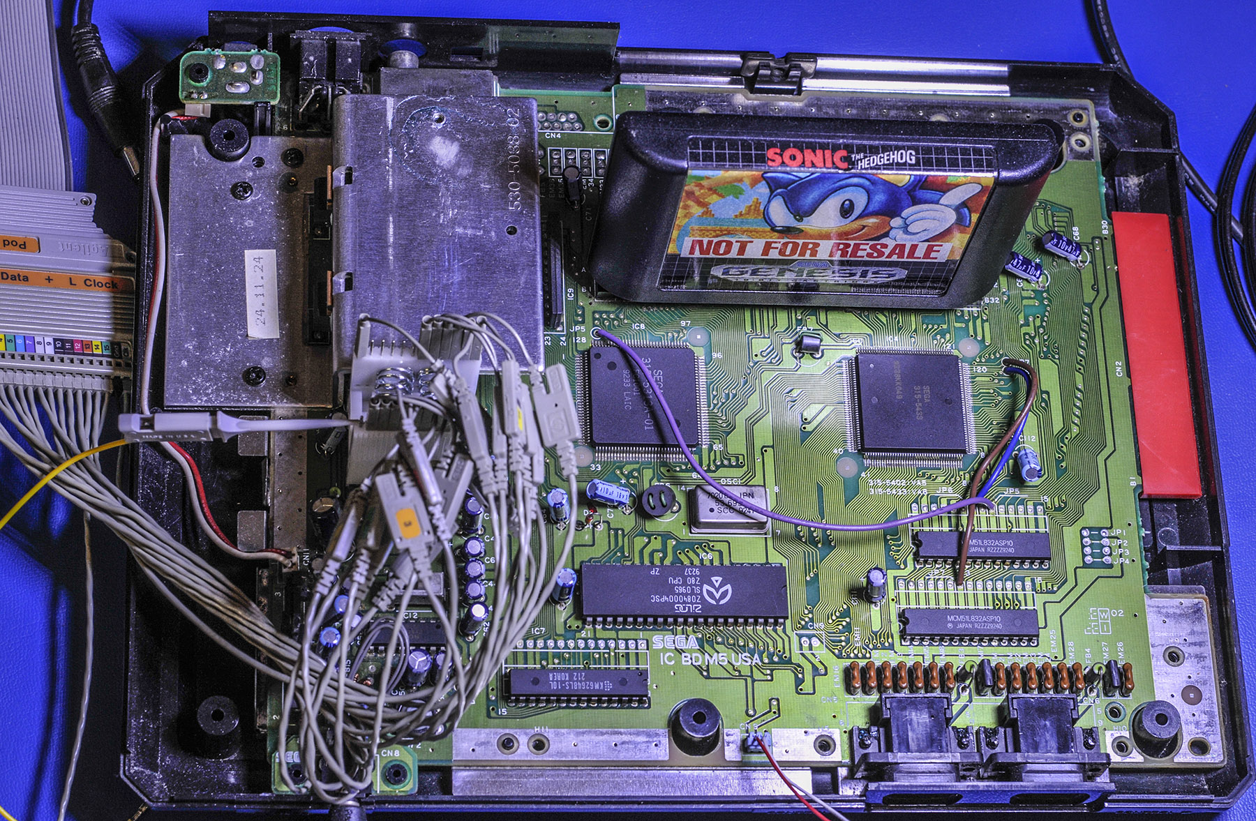
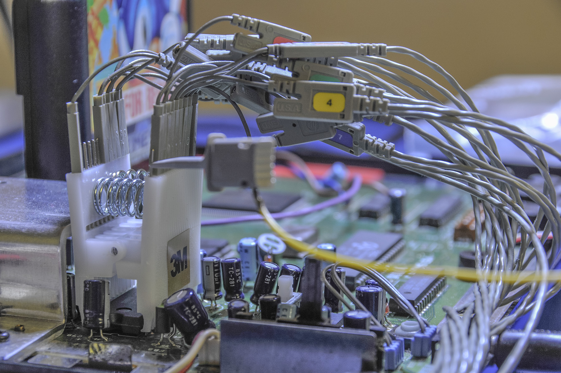
I did buy a compatible 24-pin DIP clip to make it a little easier, and a little bit more reliable, to hook up the logic analyzer.
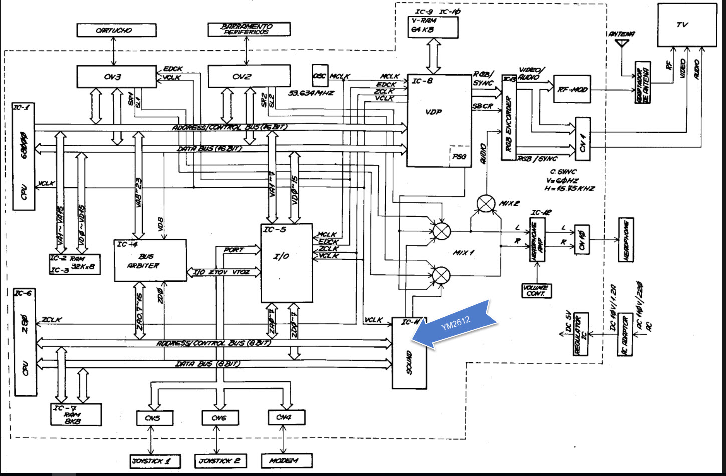
The YM2612 sits on the Z80 Bus, and so there’s lots of communication not intended directly for the YM2612’s consumption, and this data needs to be ignored.
So I setup the conditional storage logic to look at both Chip Select, but also to watch the RD_n and WR_n signals. Whatever is driving these(Z80 control, I think) has them default to HIGH (inactive, off) before they change them to the right state. This causes unnecessary invalid inputs although they do get properly ignored by the YM2612.
I also noticed that there are duplicates due to, I believe, the Z80 clock being half the frequency of the YM2612. The Z80 runs at 3.578mhz. It’s a 4mhz chip on board. The Ym2612 runs at 7.67mhz. So you’ll see repeats. I think that given the complexity of the cross-bus communication, given the arbiters, Z80, 68K, and so on changes how long things are asserted.
That’s just a theory and I haven’t dug deep enough into what documentation is available. Or really figured out the theory of operation.
Of course the music itself, the expected duration of the sound generated, and so on affect how long some of these commands stay asserted across multiple YM2612 clock cycles.
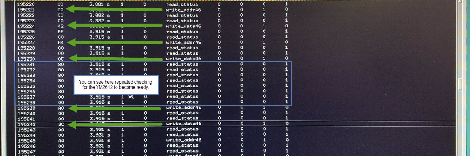
What you see below is a state-mode capture on the rising edge of the 7.67mhz clock being fed into Pin 24 of the YM2612. I’ve combined the CS, RD, WR, A1, and A0 signals into a single value I call “CtrlWord” and then assigned symbols based on the internal operation on the chip. This makes for a much more readable decode.
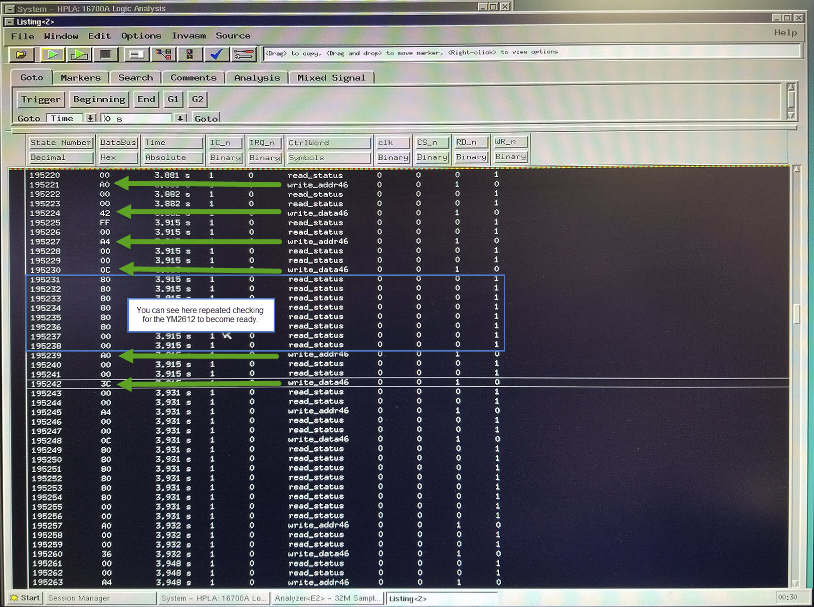
A few things that become noticeable upon inspection:
- The YM2612 has a multiplexed bus, which is usually done to save pins. Lowering the pin count lowers the manufacturing cost. And requires a smaller footprint, which also lowers PCB costs. You can see the address-first “write_addr46” command paired with the address on the data bus. Then the “write_data46” with the data coming next.
- The YM2612 is mostly unidirectional, except for reading the status byte. So mostly digital writes happen to the YM2612, which then produces analog sound output.
- You can see other devices query the YM2612’s status byte.
CAUTION: Before writing, read from any address to determine if the YM-2612 I/O is still busy from the last write. Delay until bit 7 returns to 0.
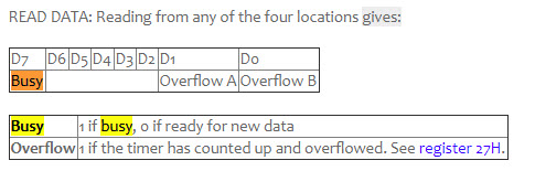
This information comes from https://www.smspower.org/maxim/Documents/YM2612.
- You can see the repeated read_status command happening, with the result coming back 0x80. This means the high-order bit is set on the byte, which means the YM2612 is busy. You can see query after query until it comes back 0. It appears some of the commands/loops have built in busy-checks happening.
So why am I doing all this anyhow? What exactly am I trying to do?
Like I may have mentioned in the previous post, I plan on adding sound to my FPGA-based tablet computer. I need sound generation aka FM Synthesis. If I can capture some sample data from a live Sega Genesis, and then feed it through the FGPA JT12 implementation, then maybe I can test it in my machine. I could also use another 68K machine for inspiration and ideas. Plus, I enjoy the process that includes some reverse engineering and figuring out how things work.

Add comment