This page seeks to share the various techniques I’ve recently employed to reverse engineer a custom PAL chip and produce a pin-compatible, equivalent function GAL chip with a goal of preserving older PCBs with failed components. It is a work-in-progress as of October 2022. Each set of topics will soon have a follow-up post where I will expand on the subject.
The various steps and strategies I used were:
- Why simply “dumping” isn’t always possible?
- Understand the system
- Create a timeline of events
- Identify your inputs and outputs
- Watch the system using a logic analyzer
- Employ statistical analysis on captures to help determine correlation between inputs and outputs
- Formulate candidate algorithms, write a python function for the chip.
- Run previous sets of data through those functions, checking for expected vs actual
- Run the previous data through the original PAL
- Write the CUPL and compile the .PLD.
- Program the .JED into the GAL.
- Run the previous data through the new GAL.
- Observe the new GAL in the destination system with a logic analyzer, debugging any issues.
- Profit!!
Three big assumptions:
- You must have a logic analyzer for this overall strategy to work. You can certainly employ some steps, but you’ll be at an information disadvantage. As you may have seen elsewhere on this site, I am a huge fan of the HP/Agilent Logic analyzers — but they are a topic and a world unto themselves. Get yourself a bus pirate, a Saleae, or similar low-cost LA. You need enough pins to cover all your inputs and outputs. For a PAL 16L8, for instance, you need approximately 18 pins.
- You must have access to a functional original PAL with the ability to remove the PAL from the system.
- While many of these techniques will work for all types of PALs, some of these will only work on L-series, so PAL16L8, for instance. Registered PALs have potentially more state available, which means that they are no longer simply a direct function on the inputs. YMMV.
What is a PAL, anyways?
Simply put, a PAL (Programmable Array logic) is a inexpensive, think under $4 in today’s overpriced world, programmable chip. This chip has a series of inputs and outputs. You describe, using hardware description languages like PALASM and CUPL, what the output pins’ state should be based on combining logic inputs using boolean algebra. Think AND, OR, or NOT.
A fantastic book on this topic is Bebop to Boolean Boogie by Maxfield. While some of his humor, is overly cheesy and not exactly my kind — his simple, clear explanations of a variety of related topics is fantastic.
An example line of CUPL:
ROM_CE = !AS_MATCH & RW & RESET;
In English, this reads, the chip enable pin of the ROM chip should be true(a logic 1), when AS_MATCH(address strobe) is 0(asserted, active low), RW is 1(a read is in progress), and RESET is one(not reset). So ROM_CE’s is one of our output pins, and the rest are the input pins. The & symbols are, well, unsurprisingly the boolean AND function. PALs are made up of usually a bunch of terms AND’d together, with an OR gate at the end, and an optional NOT gate at the output.
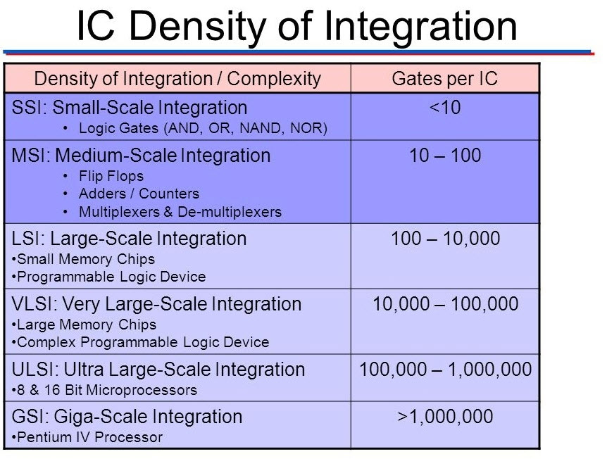
PALs replace simple, so-called SSI components, like the venerable 74-series logic chips where you may have needed dozens of chips, a larger more expensive PCB, and just a more complicated solution. PALs are further down the integration density line in the MSI to LSI range.
By definition, SSI MSI LSI and VLSI are terms used to define different orders of Digital Integrated Circuit Logic Gate Densities of Integration.
https://www.quora.com/What-are-SSI-MSI-LSI-and-VLSI?share=1
Wikipedia says it succinctly, “PAL devices have arrays of transistor cells arranged in a “fixed-OR, programmable-AND” plane used to implement “sum-of-products” binary logic equations for each of the outputs in terms of the inputs and either synchronous or asynchronous feedback from the outputs.”
I really don’t want to simply regurgitate wikipedia for the history and full description, and I won’t try. This is worth a read: https://en.wikipedia.org/wiki/Programmable_Array_Logic
Why oh why are you doing this?
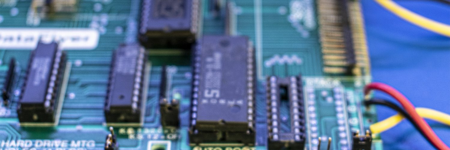
During the summer of 2022, I decided to tackle a new challenge. I had previously done a tear down and initial analysis into an HDD controller card for the Commodore Amiga called the Expansion Systems Dataflyer Plus. This card was the first one I used as a teenager, mostly from about 1991 through about 1997, whenever I bought a PC(Yuck!)
This SCSI dataflyer card has a custom PAL on it with the IDE version having two custom PALs.
While the ROMs are trivial to read, duplicate, and share, these custom programmable logic chips aren’t as easy. There’s a few reasons, which I’ll get into, on why you can’t simply read them. So you need to employ a fair bit of analysis and deductive reasoning to reverse engineer them.
Someone commented on a previous post about making the logic on those PALs available, and so I decided to tackle this problem. It was on my bucket list to get “down and dirty” with the PALs, and exactly what I did.
For what it’s worth, I simply hate the idea of this older technology dying. I fully understand that newer, better HDD controllers for the Amiga’s exist. I don’t care. I want to preserve this technology, as it was, so that when a custom chip dies, it doesn’t kill the whole board. There’s no reason, using all of the tools and technologies we have available today, not to take the time to preserve our early computing history. The 1980s and 1990s were special to me. The computers and their accessories helped form the foundation of who I am today — and if I can do my part to ensure that foundation is taken care of.
I’m a student of life like all of you, and have no formal training, education, or much work-related experience in this particular area. It took me weeks to a couple months to figure some of this stuff out, and so I thought I’d share my experience to help speed you along with your project!


[…] Reverse Eng’ing PALs […]
[…] Reverse Eng’ing PALs […]
I love reading your blog and am getting especially excited that someone is reverse engineering an Amiga SCSI controller. My friend Chris and I have done a similar thing: https://www.scsi.me/ (ReAmiga 4091) and, we also were puzzled by the GALs, although we were lucky and could use the PLD source code released by Dave Haynie.
Chris developed Brutus28 to help unlocking GAL secrets: https://github.com/cdhooper/brutus28
Hey Stefan,
Thanks for your comment! I did find your project probably about six months ago or so. I think I watched a few minutes of one of the talks as well.
Great job on the project — the PCB looks sweet with the gold on black!
I see you use the NCR 53C710 — I’ve got a couple points of crossover with your project! I also hack around on an HP-UX based logic analyzer which uses a soft-core 53C710 embedded in custom silicon. I’m pretty sure HP, for good reasons I’m sure, handicapped the SCSI core though to 5MB/s. I was optimizing boot times and general overall performance, so I was tracking down bottlenecks.
https://www.techtravels.org/2019/12/effects-of-upgrading-scsi2sd-from-v5-4-8-3-to-v6-6-2-1-analysis-hp-16700a/
One of my several unfinished projects include introducing a new, faster SCSI card to that logic. There’s a custom connector for the internal 33mhz PCI bus, which I started to build an adapter for.
Yeah the PAL/GAL re’ing efforts are a heck of a lot simpler whenever they are straight combinatorial, and the introduction of even a couple bits of state, via latches, makes it harder. This is why I started that blog series on RE’ing.
Glad you reached out! Great job again!
[…] Reverse Eng’ing PALs […]