Ok, so I’ve finally got some work done on this tonight.
I’ve decided to go to a 4-line buffer system because it’s a more round number than 3 — makes everything easier to deal with.
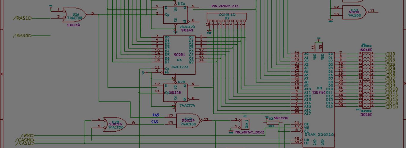
I’ve gotten rid of the dram controller, and all associated circuitry. Create (4) dual-port rams, instantiated my amiga video acquisition module.
Good progress tonight. Still have to create the write FSM for grabbing the data from the amiga module and writing it into the correct line buffer. Should be easy but at 1:33am local time, I’ve got to sleep.
I wanted to keep the work modularized and so I needed what I believe is called a (one-hot?) decoder — which takes a single write enable signal, and a 2-bit select signal for the write bank, and then outputs four separate signals so that only one of the signals is enabled at a time. All are sitting on standby, but only one line buffer will only be written to, every 320 pixels. All are being fed an x-coordinate for a write address.
I haven’t had a chance to simulate this, but I think it’ll work. Here’s my code:
[cc lang="verilog"]module wren_decoder(

select,

bank_wrens,

master_wren

);
input [1:0] select;
input master_wren;
output reg [3:0] bank_wrens ;
always @ (select or master_wren)
begin
if (master_wren) begin
case (select)
2’d0 : bank_wrens = 4’b0001;
2’d1 : bank_wrens = 4’b0010;
2’d2 : bank_wrens = 4’b0100;
2’d3 : bank_wrens = 4’b1000;
endcase
end
else begin
bank_wrens = 4’b0000;
end
end
endmodule[/cc]
If master_wren is disabled, then all four rams see wr_enable disabled.
If master_wren is enabled, then based on the bank selection, the correct ram is enabled for writing.
Each ram gets their wr_enable signal tied to bank_wrens[0], bank_wrens[1], and so on……
Look ok?
Add comment